An Introduction to Field Programmable Gate Arrays
A field programmable gate array (FPGA) is a "blank slate" circuit. Think of an FPGA like a huge box of LEGOs. An FPGA lets you build almost any digital device you imagine, unlike a pre-built toy car that cannot change. This flexibility makes field programmable gate arrays powerful tools for everything from prototyping new technologies to accelerating tasks in data centers. The importance of field programmable arrays is growing rapidly, as shown by market projections.
| Metric | Value |
|---|---|
| Estimated Market Size (2024) | USD 12.1 billion |
| Projected Market Size (2029) | USD 25.8 billion |
| CAGR (2025-2029) | 16.4% |
Key Takeaways
- An FPGA is a special computer chip. You can change what it does after it is made. This is like building different things with the same LEGOs.
- FPGAs are reprogrammable. They can fix problems or add new features easily. You just load a new set of instructions onto the chip.
- FPGAs are good at doing many tasks at once. This is called parallelism. They are faster than regular computer chips for some jobs.
- FPGAs save money and time. They let you test new ideas without making expensive custom chips. This helps create new products faster.
- FPGAs are used in many places. They help make 5G phones work. They also speed up computers in data centers and help NASA explore Mars.
What is a Field Programmable Gate Array?
To understand this technology, one can break down its name. "Field Programmable" means a user or designer can configure the chip's function after it leaves the factory, out in the "field." This is different from most chips, which have a permanent, unchangeable function. The term "Gate Array" refers to the chip's internal structure: a massive grid of generic logic gates and memory. These components are not connected until a designer loads a configuration file.
The history of the modern field programmable gate array began in 1985. Ross Freeman and Bernard Vonderschmitt, co-founders of the company Xilinx, introduced the first commercially successful version, the XC2064. Ross Freeman's idea of a chip with reconfigurable logic was so important that he was later inducted into the National Inventors Hall of Fame for it.
The Reprogrammable Integrated Circuit
The core identity of an FPGA is its ability to be reprogrammed. Each time an SRAM-based FPGA powers on, it is a blank slate. The device then enters a configuration mode. During this mode, a special file called a "bitstream" is loaded from an external memory source onto the chip. This bitstream acts like a set of instructions, telling the chip how to connect its internal gates to create the desired digital circuit.
This entire process happens automatically and very quickly. The key steps are:
- Power-Up: The system powers on, and the FPGA prepares itself. It is initially unconfigured.
- Configuration: The FPGA downloads the bitstream. This file configures the internal logic and connections. The device is now ready to operate.
If a designer needs to fix a bug or add a new feature, they simply create a new bitstream and reload it. This makes the FPGA a truly reprogrammable logic device, offering incredible flexibility for development and updates.
A Sea of Logic Gates
Inside an FPGA lies a vast, orderly grid of components. The most fundamental of these are called Look-Up Tables, or LUTs. A LUT is a tiny piece of memory that can be programmed to act like any simple logic gate. It works by storing a truth table. The inputs to the LUT act as an address to look up the correct output value from its memory.
💡 How a LUT Works: An Example A simple 2-input LUT can become an AND gate. The designer programs its memory to store the results for every possible input.
- If inputs are
00, the output is0.- If inputs are
01, the output is0.- If inputs are
10, the output is0.- If inputs are
11, the output is1. The LUT simply looks up the correct pre-stored answer for any given input.
An FPGA contains thousands or even millions of these LUTs, along with other elements like flip-flops for storing data. These elements are the "sea of gates" waiting for a design to give them purpose.
Hardware You Can Redesign
Designers do not draw circuits by hand to create a configuration for an FPGA. Instead, they describe the hardware's behavior using a special programming language. These are called Hardware Description Languages (HDLs). The two most common HDLs are:
- VHDL
- Verilog
More recently, High-Level Synthesis (HLS) tools have emerged. These tools allow designers to use familiar languages like C++ or OpenCL to describe their hardware, making field programmable arrays more accessible. The general design flow follows a clear path from code to a functional chip.
- RTL Coding: A designer writes code in an HDL to describe the circuit's function.
- Synthesis: A software tool translates the HDL code into a list of digital logic components, like LUTs and flip-flops.
- Implementation: The software then figures out the best way to place these components on the FPGA and route the wires between them.
- Bitstream Generation: The tool converts the final, implemented design into the binary
bitstreamfile. - Program FPGA: Finally, the designer loads this bitstream onto the field programmable gate array, bringing the custom digital circuit to life.
Inside an FPGA: Core Components
An FPGA contains three main types of resources that work together. These components are the configurable logic blocks, the programmable interconnects, and the input/output blocks. A designer's bitstream file configures all three to create a custom hardware circuit.
Configurable Logic Blocks (CLBs)
The core building blocks of an fpga are the configurable logic blocks (CLBs). These are small, identical units repeated thousands of times across the chip. Each CLB is a versatile toolkit for creating digital logic. A typical CLB contains several key components:
- Look-up Tables (LUTs): These perform most logic functions.
- Flip-Flops: These are single-bit memory cells that store data.
- Multiplexers: These circuits select between different signal inputs.
Flip-flops are especially important for creating sequential logic. They act as binary shift registers, saving a logic state (a 1 or a 0) between cycles of a clock signal. This ability to store information allows a designer to build circuits like counters and state machines directly on the fpga.
Programmable Interconnects
Programmable interconnects form a complex routing fabric. This fabric is a dense network of wires that runs between all the CLBs on the chip. It acts like a programmable switchboard. When the fpga loads its bitstream, the file dictates exactly how to connect these wires. The interconnects create pathways that link the outputs of some CLBs to the inputs of others, wiring them together to form the larger, complete circuit. This routing is just as critical as the logic inside the CLBs.
Input/Output (I/O) Blocks
Input/Output (I/O) blocks sit at the perimeter of the chip. They act as the interface between the internal logic of the FPGA and the outside world. These blocks are highly configurable. A designer can program them to support different electrical standards and voltages.
Modern Connectivity 🚀 Many modern FPGAs include specialized, high-speed I/O transceivers. These hardened blocks allow the device to communicate directly using fast serial protocols like PCIe and Ethernet without using up general logic resources.
These powerful I/O capabilities make it possible to connect an FPGA to a wide range of other components, from simple sensors to high-performance computer systems.
FPGA vs. Other Chips
An FPGA offers unique advantages, but it is not the only type of processing chip. Understanding how an FPGA compares to other common chips helps a designer choose the right tool for the job. The main competitors are CPUs, GPUs, and ASICs.
Parallelism: FPGA vs. CPU
A Central Processing Unit (CPU) is the brain of a traditional computer. It excels at performing complex tasks one after another very quickly. A CPU follows a list of instructions sequentially. An FPGA, however, works differently. It is a master of true parallelism. A designer can configure an FPGA to perform thousands of simple tasks all at the same time.
- CPU: A CPU processes instructions sequentially. It uses a technique called pipelining to work on different stages of several instructions at once. This increases its efficiency but it is still fundamentally a sequential device.
- FPGA: An FPGA achieves higher throughput by laying out operations in physical space on the chip. This creates a deep hardware pipeline. New data can enter this pipeline every single clock cycle. This spatial parallelism eliminates the control overhead found in a CPU.
Studies comparing performance for tasks like image filtering and stereo-vision often show the strength of an FPGA. Researchers use CPUs as a baseline to measure the performance gains from the parallel architectures of FPGAs and GPUs. The FPGA's ability to handle many data streams at once makes it ideal for real-time signal processing and video analysis.
Customization: FPGA vs. GPU
A Graphics Processing Unit (GPU) is also a parallel processor. It contains thousands of simple cores designed to perform the same operation on large blocks of data. This structure makes GPUs excellent for graphics rendering and machine learning. However, a GPU has a fixed parallel architecture. A designer cannot change its fundamental layout.
An FPGA offers fully customizable parallelism. The designer defines the entire hardware architecture, from the individual logic operations to the data paths between them. This customization provides a key advantage in power efficiency. GPUs deliver incredible computing power but often consume a lot of energy. An FPGA, optimized for a specific application, uses less power. This makes the FPGA a great choice for tasks where energy efficiency is more important than raw processing speed.
Flexibility: The Value of Field Programmable Arrays
The most important comparison for many product developers is between field programmable arrays and the application-specific integrated circuit (ASIC). An ASIC is a chip designed for one single purpose. It is the fastest and most power-efficient option for that specific task.
ASIC: The ultimate in performance, but with zero flexibility. Once an ASIC is manufactured, its function can never be changed.
Creating an ASIC involves a massive upfront cost called Non-Recurring Engineering (NRE). These NRE costs cover the entire design and verification process, along with the expensive tooling required for manufacturing. These costs can easily run into hundreds of thousands or even millions of dollars.
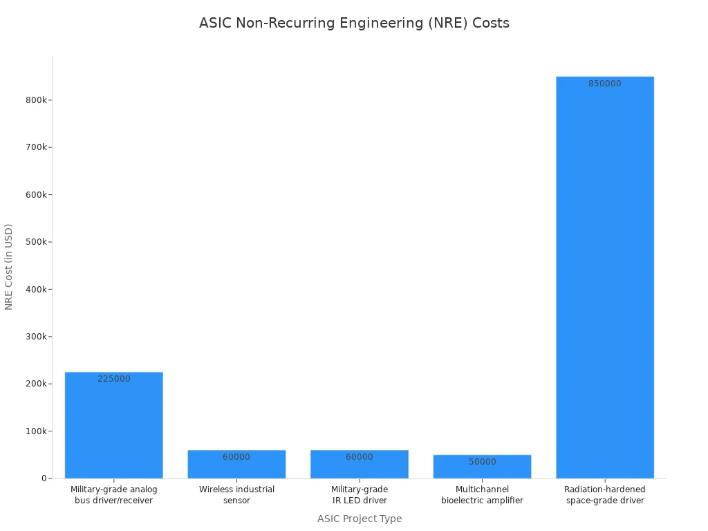
| Project Description | Typical NRE Cost |
|---|---|
| Wireless Industrial Sensor | $60,000 |
| Military-Grade Driver | $225,000 |
| Space-Grade Power Driver | $850,000 |
This is where field programmable arrays shine. An FPGA is an off-the-shelf component with no NRE costs. It provides total flexibility. A designer can prototype a system, fix bugs, and add features by simply loading a new bitstream. This makes the fpga the perfect solution for:
- Prototyping ASIC designs before committing to manufacturing.
- Products with low to medium production volumes.
- Applications where standards may change or updates are needed after deployment.
Real-World FPGA Applications
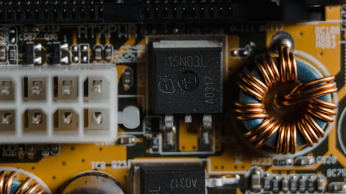
The unique flexibility of FPGAs makes them essential tools across many advanced industries. Their ability to be reconfigured allows them to solve problems that other chips cannot handle as efficiently.
Prototyping and Emulation
Developers often use FPGAs to build and test prototypes of new ASIC designs. This process, called emulation, allows them to find and fix bugs in the hardware design before committing to the expensive manufacturing of an ASIC. This saves millions of dollars and months of development time.
Data Center Acceleration
Modern data centers use FPGAs to speed up demanding workloads like machine learning and data analytics. Major cloud providers offer FPGA-based services to their customers.
For example, Amazon Web Services (AWS) provides EC2 F1 and F2 instances that use FPGAs. Other providers like Microsoft Azure and Alibaba Cloud also give users access to reconfigurable hardware for custom acceleration.
Telecommunications and 5G
FPGAs are critical components in telecommunications infrastructure, especially for 5G networks. They perform intensive digital signal processing tasks in real time. These tasks include:
- High-performance Fast Fourier Transform (FFT) engines.
- AI-based channel estimation to improve signal reliability.
- Data formatting and packet formation.
Aerospace and Defense
In aerospace and defense, systems require reliability in extreme environments. Manufacturers create special radiation-hardened FPGAs for this purpose. NASA used reprogrammable FPGAs on its Mars rovers for critical landing and mobility functions. The military also uses the fpga in Software-Defined Radio (SDR) systems. This technology allows communication devices to adapt to new protocols and frequencies on the fly.
High-Performance Computing
Scientists use FPGAs to accelerate complex research computations. In genomics, an FPGA-based accelerator for nanopore sequencing achieved a speedup of over 10 times compared to a CPU. This technology also speeds up other scientific problems, including:
An FPGA is a uniquely flexible and reprogrammable chip that excels at parallel processing. Its main advantages are reconfigurability and custom hardware acceleration. This design allows developers to bring products to market much faster than with custom-made chips. An FPGA lets them test ideas, fix bugs, and add features without expensive manufacturing delays. These field programmable arrays are more than just components.
They are powerful platforms for innovation. An FPGA enables engineers to build custom hardware solutions for the world's most complex problems.
FAQ
💡 How much does an FPGA cost?
The cost of an FPGA varies greatly. Small boards for hobbyists and students can cost less than $100. High-end FPGAs for data centers or aerospace applications can cost thousands of dollars. The price depends on the chip's size, speed, and features.
💻 Is programming an FPGA difficult?
Programming an FPGA requires a different mindset than software development. Designers use Hardware Description Languages (HDLs) like Verilog or VHDL. These languages describe hardware circuits. Learning HDL can be challenging, but new tools that use C++ or Python are making it easier for beginners.
🐍 Can I use Python to program an FPGA?
Yes, a designer can use Python to program an FPGA. Special frameworks like PYNQ or Amaranth allow developers to use Python. These tools convert the Python code into a hardware design. This makes FPGA technology more accessible to software developers and researchers.
💰 When should I choose an FPGA over a microcontroller?
A designer chooses an FPGA for tasks needing high-speed parallel processing. Microcontrollers are better for sequential tasks and simple control logic. Use an FPGA for video processing or high-frequency signal analysis. Use a microcontroller for reading sensors or controlling motors.