What Makes NPN and PNP Transistor Symbols Unique
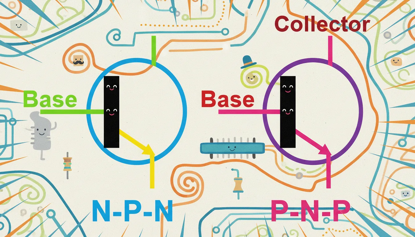
The easiest way to tell NPN and PNP transistors apart is by looking at the arrow on the transistor symbol. The direction of this arrow, found on the emitter, shows you which way the conventional current flows. If you spot the arrow pointing out, you are looking at an NPN transistor. If it points in, you have a PNP transistor. Electronics textbooks often highlight this arrow as the main difference and link it to how the transistor works inside. Recognizing this small detail helps you avoid mistakes in circuit design and troubleshooting.
Key Takeaways
The arrow on the emitter is the fastest way to tell NPN and PNP transistors apart: arrow points out for NPN, in for PNP.
The arrow shows the direction of conventional current flow, helping you understand how the transistor works in a circuit.
NPN transistors use electrons as charge carriers and have an outward arrow; PNP transistors use holes and have an inward arrow.
Correctly identifying the transistor symbol prevents wiring mistakes and ensures your circuit works as intended.
Using the mnemonics 'Not Pointing iN' for NPN and 'Pointing iN Proudly' for PNP helps you remember the arrow directions easily.
Transistor Symbol Structure
Terminals: Base, Collector, Emitter
Every transistor symbol shows three main parts: the base, the collector, and the emitter. These terminals appear in both NPN and PNP types. You can think of the base as the control gate. It decides when the transistor turns on or off. The collector acts like a collector of current, while the emitter sends out or receives current, depending on the type.
Here is a table that shows how each terminal appears in the NPN and PNP transistor symbol:
Component | NPN Transistor Symbol Representation | PNP Transistor Symbol Representation |
|---|---|---|
Emitter (E) | Arrow points away from the base towards the emitter | Arrow points towards the base and away from the emitter |
Base (B) | Central reference point in the symbol | Central reference point in the symbol |
Collector (C) | Positioned opposite the emitter, completing the three-layer symbol | Positioned opposite the emitter, completing the three-layer symbol |
The base controls the transistor. In an NPN bjt, a small current into the base lets a larger current flow from collector to emitter. In a PNP bjt, a small current leaving the base allows a larger current to flow from emitter to collector. The emitter always acts as the source of charge carriers. In NPN, it sends out electrons. In PNP, it sends out holes.
Arrow Direction Meaning
The arrow on the emitter in a transistor symbol is not just for decoration. It tells you the direction of conventional current flow. For NPN, the arrow points out of the emitter. This means current flows from the collector to the emitter. For PNP, the arrow points into the emitter, showing current flows from emitter to collector.
Tip: The arrow direction matches the direction of current in the base-emitter junction when the transistor is on.
You can use these mnemonics to remember the arrow direction:
NPN: "Not Pointing In" (arrow points out)
PNP: "Pointing In Proudly" (arrow points in)
This simple trick helps you quickly tell which bjt symbol you see in a circuit.
NPN Transistor Symbol
NPN Symbol Features
When you look at an npn transistor symbol, the first thing you notice is the arrow on the emitter. This arrow points outward, away from the base. The outward-pointing arrow shows you the direction of conventional current flow when the npn transistor is active. This feature makes it easy to tell an npn from a pnp transistor in any circuit diagram.
The arrow on the emitter points out, showing current flows out of the emitter terminal.
This arrow helps you quickly spot an npn transistor and not confuse it with a pnp type, where the arrow points in.
The arrow also matches the direction of electron flow inside the device, which is a key part of how the npn bjt works.
The npn transistor symbol also reflects its internal structure. You have a thin P-type layer (the base) sandwiched between two N-type layers (the emitter and collector). The emitter is heavily doped with N-type material, making it a strong source of electrons. The base is thin and lightly doped, which lets most electrons pass through to the collector. This layered design is why the arrow points outward on the symbol.
Tip: Remember, "Not Pointing iN" helps you recall that the npn arrow points out!
NPN Current Flow
You can understand how an npn transistor works by following the current flow in a circuit. The base is positive compared to the emitter, and the collector is even more positive. When you apply a small current to the base, it allows a much larger current to flow from the collector to the emitter.
The emitter is forward biased relative to the base, so electrons move from the emitter into the base.
Most electrons travel through the thin base and reach the collector, forming the main collector current.
Only a small number of electrons combine in the base, so the base current stays small.
The emitter current equals the sum of the collector and base currents (IE = IC + IB).
The arrow on the npn transistor symbol points outward, showing conventional current flows out of the emitter terminal.
In circuit diagrams, the collector connects to a positive voltage, and the base is also positive compared to the emitter.
Npn transistors are popular in many circuits because electrons, the main charge carriers, move quickly. You often see npn transistors in amplifiers, switches, and sensors. The symbol's outward arrow matches their role as current sinks, making them easy to use in switching and amplification tasks.
Feature | NPN Transistor Symbol |
|---|---|
Arrow Direction | Outward from emitter |
Layer Structure | N-P-N |
Main Charge Carriers | Electrons |
Common Applications | Amplifiers, switches, sensors |
PNP Transistor Symbol
PNP Symbol Features
When you look at a pnp transistor symbol, you will see the arrow on the emitter pointing inward, toward the base. This arrow is the most important feature that sets the pnp apart from the npn type. The inward-pointing arrow shows you the direction of conventional current flow. In a pnp transistor, current flows from the emitter into the base. This is the opposite of what you see in an npn transistor, where the arrow points out.
The pnp transistor symbol also tells you about its internal structure. The layers are arranged as Positive-Negative-Positive, or P-N-P. The emitter and collector are both made of P-type material, while the base is N-type. The emitter in a pnp bjt is heavily doped with P-type material, which means it has lots of holes, or positive charge carriers. These holes move from the emitter into the base when the transistor is active.
Tip: Remember, "Pointing iN Proudly" helps you recall that the pnp arrow points in!
Here is a quick table to help you compare the pnp and npn transistor symbols:
Feature | PNP Transistor Symbol | NPN Transistor Symbol |
|---|---|---|
Arrow Direction | Inward (toward base) | Outward (away from base) |
Layer Structure | P-N-P | N-P-N |
Main Charge Carriers | Holes | Electrons |
PNP Current Flow
You can understand how a pnp transistor works by following the current flow. The arrow on the emitter points inward, showing that conventional current enters the emitter and moves toward the base. In a pnp transistor, the emitter is at a higher voltage than the base and collector. When you apply a small current leaving the base, it allows a larger current to flow from the emitter to the collector.
The pnp bjt uses holes as the main charge carriers. These holes move from the P-type emitter into the N-type base. Most of the holes pass through the base and reach the collector, creating the main collector current. Only a small number of holes combine in the base, so the base current stays small. The emitter current equals the sum of the collector and base currents (IE = IC + IB), just like in an npn bjt.
Note: The inward arrow on the pnp transistor symbol always shows the direction of conventional current flow, from emitter to collector. This helps you avoid confusion when reading circuit diagrams.
You will often use pnp transistors in circuits where you need to switch the positive side of the power supply. The unique symbol makes it easy to spot a pnp in any schematic. By understanding the arrow direction and the layer structure, you can quickly identify and use pnp transistors in your projects.
NPN vs PNP: Symbol Comparison
Arrow Direction Summary
When you compare npn and pnp transistor symbols, the arrow on the emitter stands out as the most important feature. This arrow tells you the direction of conventional current flow. In an npn transistor, the arrow points away from the base. This means current flows out of the emitter. In a pnp transistor, the arrow points toward the base, showing current flows into the emitter. You can spot this difference quickly in any schematic.
Electronics standards around the world, like IEC 60617 and IEEE Standard 315, use this arrow direction to define each transistor symbol. These standards make sure you see the same symbol in textbooks, circuit diagrams, and ECAD software. The arrow direction is not just a drawing detail. It helps you understand how the transistor works in a circuit.
Tip: The arrow always points in the direction of conventional current. For npn, it points out. For pnp, it points in.
You can use simple mnemonics to remember this:
For npn: "Not Pointing iN" (arrow points out)
For pnp: "Pointing iN Proudly" (arrow points in)
This trick helps you avoid mistakes when reading or drawing circuit diagrams.
Quick Reference Table
You can use the table below to compare npn vs pnp transistor symbols at a glance. This table highlights the key visual differences and the direction of current flow.
Feature | NPN Transistor Symbol | PNP Transistor Symbol |
|---|---|---|
Arrow Direction on Emitter | Points away from the base | Points towards the base |
Conventional Current Flow | From collector to emitter | From emitter to collector |
Mnemonic | Not Pointing iN | Pointing iN Proudly |
Main Charge Carriers | Electrons | Holes |
Symbol Appearance | Arrow out, base in the middle | Arrow in, base in the middle |
The emitter arrow is the fastest way to tell npn from pnp.
Both types have three leads: base, collector, and emitter.
The physical pin order can look like a mirror image between npn and pnp, even if the pin names stay the same.
Remember: The arrow on the emitter is your best guide. If you see it pointing out, you have an npn. If it points in, you have a pnp.
This quick reference helps you read any transistor symbol with confidence. You can now identify npn vs pnp in seconds, which makes your circuit design and troubleshooting much easier.
Why Symbol Differences Matter
Circuit Design Impact
You need to recognize the correct transistor symbol when you design or repair circuits. The arrow direction on the emitter tells you if you are working with an npn or a pnp device. This small detail changes how you connect the transistor and how current flows in your project. If you use the wrong symbol, your circuit may not work as expected.
When you look at npn and pnp transistors, you see that each type has a unique role. Npn transistors usually handle low-side switching, where the emitter connects to ground. Pnp transistors often work in high-side switching, with the emitter tied to the positive supply. The symbol helps you choose the right type for your application.
Here is a table that shows how correct symbol identification affects troubleshooting and design:
Aspect | NPN Transistor | PNP Transistor |
|---|---|---|
Symbol Arrow Direction | Outward arrow indicating current flow from collector to emitter | Inward arrow indicating current flow from emitter to collector |
Base-Emitter Biasing | Base voltage positive relative to emitter (forward biased) | Base voltage negative relative to emitter (forward biased) |
Current Flow Direction | Collector to emitter when base is positive | Emitter to collector when base is negative |
Majority Charge Carriers | Electrons | Holes |
Typical Circuit Configuration | Low-side switching (emitter grounded) | High-side switching (emitter connected to positive supply) |
Impact on Troubleshooting | Correct symbol identification ensures proper understanding of current flow, biasing, and switching behavior, which is critical for diagnosing faults | Misidentification leads to incorrect assumptions about current direction and biasing, reducing troubleshooting success |
Application Context | Common in digital logic and high-speed switching | Used in analog circuits and positive voltage switching |
Tip: Always double-check the arrow direction before placing a transistor in your circuit. This habit saves you time and prevents errors.
Common Mistakes
Many beginners confuse npn and pnp symbols. You might see a circuit fail because the wrong transistor type was used. If you mix up the symbols, you could reverse the current flow or bias the base incorrectly. This mistake can stop a circuit from working or even damage components.
Some common errors include:
Placing an npn transistor where a pnp should go, or vice versa.
Ignoring the arrow direction and connecting the base or emitter to the wrong voltage.
Forgetting that npn and pnp devices have different majority charge carriers (electrons for npn, holes for pnp).
When you work with bipolar transistors, always check the symbol. The arrow direction gives you a quick clue. If you remember this, you will avoid most mistakes with bipolar junction transistors. You will also find troubleshooting much easier, since you know how current should flow.
Note: Careful symbol reading helps you build reliable circuits and fix problems faster. Practice spotting the differences every time you see a transistor symbol.
You can quickly spot the difference between NPN and PNP symbols by checking the arrow on the emitter:
NPN: Arrow points away from the base.
PNP: Arrow points toward the base.
This arrow shows the direction of current flow and helps you avoid mistakes in real circuit schematics. Practice reading these symbols in actual diagrams to build your skills. Next, learn how transistors work by building simple circuits, reading trusted books, and using simulation tools.
FAQ
What is the fastest way to tell NPN and PNP transistor symbols apart?
Look at the arrow on the emitter. If the arrow points out, you have an NPN transistor. If it points in, you have a PNP transistor. This arrow shows the direction of conventional current flow.
Why does the arrow direction matter in a circuit?
The arrow direction tells you how current flows through the transistor. If you connect the transistor the wrong way, your circuit will not work. Always match the symbol to the correct transistor type.
Can you use NPN and PNP transistors in the same circuit?
Yes, you can use both types together. Many circuits use NPN and PNP transistors to create push-pull stages or to handle different switching needs. Make sure you connect each one correctly.
What happens if you mix up NPN and PNP transistors?
Your circuit may not turn on.
You could damage the transistor.
Current might flow in the wrong direction.
Always double-check the symbol and the part before you build your circuit.
Do the physical pins match the symbol layout?
Not always. The symbol shows the function, not the pin order. Check the datasheet for the exact pinout of your transistor before soldering or connecting it.