How Are PCBs Assembled A Step by Step Breakdown
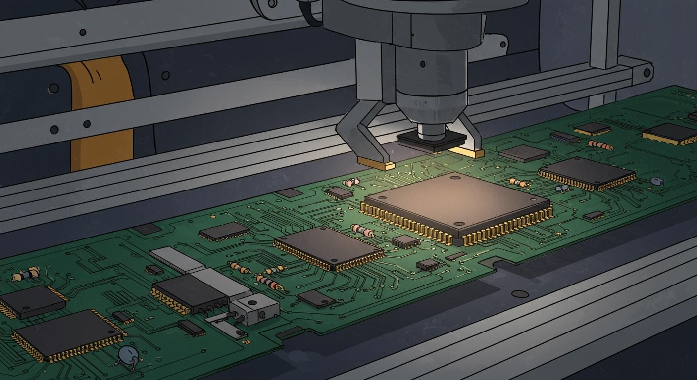
You start the circuit board assembly process with a bare board. The goal is to turn it into a functional electronic brain. This involves mounting all the necessary electronic components onto the PCB.
PCB assembly is the process of soldering electronic components onto a printed circuit board (PCB).
Manufacturers use two main methods for this printed circuit board assembly:
- Surface Mount Technology (SMT)
- Through-Hole Technology (THT)
The pcb assembly process follows a precise sequence of steps. It moves from solder application to final testing, ensuring each PCB works perfectly. The industry's growth highlights its importance.
| Year | Market Size (USD Billion) | CAGR (2025-2035) |
|---|---|---|
| 2023 | 36.86 | N/A |
| 2024 | 39.45 | N/A |
| 2035 | 57.24 | 3.44% |
Key Takeaways
- PCB assembly turns a bare board into a working electronic part. It involves placing and soldering electronic components onto the board.
- Manufacturers use two main ways to put parts on a PCB: Surface Mount Technology (SMT) for small parts on the surface, and Through-Hole Technology (THT) for larger parts that go through holes.
- The assembly process starts with checking design files and applying solder paste. Then, machines place components with great accuracy.
- After placing parts, soldering melts the paste to connect them. Reflow soldering is for SMT parts, and wave soldering is for THT parts.
- The final steps include checking the board for mistakes, cleaning it, and testing it to make sure it works correctly.
The PCB Assembly Process Kickoff
Before any components touch a board, your design files undergo a critical review. This is the first step in the circuit board assembly process. Manufacturers perform Design for Manufacturability (DFM) checks. These checks ensure your PCB design is optimized for a smooth manufacturing process. They review aspects like component placement, thermal management, and material selection to prevent issues later.
Your design data provides the blueprint for the entire pcb assembly. You must supply a complete set of files.
| File Name | Description |
|---|---|
| Gerber/ODB++/IPC-2581 | Contains the layout data for each PCB layer. |
| Bill of Materials (BOM) | Lists every component, part number, and quantity. |
| Centroid File | Provides the X-Y coordinates for automated component placement. |
Pro Tip: Modern formats like ODB++ and IPC-2581 bundle all necessary data into a single file. This simplifies the data transfer and reduces the risk of errors compared to the multi-file Gerber format.
Solder Paste Stenciling
With the design verified, the first hands-on step of the pcb assembly process begins. You apply solder paste to the bare PCB. A thin, stainless steel stencil is placed over the board. The stencil has small, laser-cut holes that align perfectly with the component pads on the PCB. A squeegee blade sweeps a layer of solder paste across the stencil. This deposits the paste precisely onto the pads where components will be soldered. The type of paste used, such as lead-free SAC305 or a no-clean formula, depends on the product's specific requirements.
Component Procurement
While the bare boards are prepared, your manufacturer sources all the necessary electronic components. This stage relies on an accurate Bill of Materials (BOM). Verifying the BOM is crucial to prevent sourcing errors like incorrect part numbers or quantities. Sourcing authentic components is a major challenge. The global supply chain makes it difficult to avoid counterfeit parts, especially for end-of-life (EOL) components that are no longer in production. A reliable pcb assembly partner works with vetted suppliers to ensure every part is genuine and meets quality standards.
Core Printed Circuit Board Assembly
After preparing the files and applying solder paste, you reach the heart of the printed circuit board assembly. This is where your bare board begins its transformation. Components are carefully placed onto the PCB using one of two primary methods: Surface Mount Technology (SMT) or Through-Hole Technology (THT). The choice depends on the type of components your design requires.
SMT Component Placement
Surface Mount Technology is the most common method used in modern electronics. You place surface mount components directly onto the pads of the PCB where you previously applied solder paste. These components, called Surface Mount Devices (SMDs), do not have long leads that pass through the board. Instead, they have small metal contacts that sit flat on the surface. This allows you to fit more components into a smaller space.
The key difference between SMT and THT is how components interact with the board. SMT components sit on the surface, while THT components go through it.
This table breaks down the main distinctions:
| Feature | Surface Mount Technology (SMT) | Through-Hole Technology (THT) |
|---|---|---|
| Component Type | Surface Mount Devices (SMDs) | Through-hole components |
| Leads/Contacts | Small metal or ceramic contacts | Long wire leads |
| PCB Interaction | Placed directly onto pads | Leads inserted into drilled holes |
| Size | Generally much smaller and lighter | Generally larger and heavier |
Because SMDs are smaller and lighter, they are perfect for compact devices like smartphones and wearables.
Automated Pick-and-Place
You use an automated pick-and-place machine to perform SMT placement with incredible speed and precision. This robotic device is the workhorse of the pcb assembly line. It uses the Centroid file from your design data to know the exact X-Y coordinates and rotation for every single component.
The machine's vision system acts as its eyes, ensuring flawless placement. 🤖 Here is how it achieves such high accuracy:
- PCB Mapping: A camera first scans the PCB to find fiducial marks. These are small markers on the board that serve as reference points for perfect alignment.
- Component Detection: As the machine picks up a component from its reel, another camera takes a picture. The system analyzes the component's shape, size, and orientation.
- Positioning Analysis: The software compares the component's current position to the required position on the board.
- Real-Time Correction: If a component is slightly off-center on the nozzle, the machine adjusts its placement path to compensate. This happens in milliseconds.
Modern machines can achieve micron-level accuracy, which is essential for placing tiny components.
| Component Type | Required Accuracy |
|---|---|
| 01005 (0.4mm x 0.2mm) | 0.05 mm |
| High-precision machines | Micron level (0.001 mm) |
This automation allows for the placement of thousands of components per hour, a task impossible to do by hand.
THT Component Insertion
Through-Hole Technology is an older but still essential method. It is used for components that require a stronger mechanical bond to the PCB. These components have long wire leads that you insert through holes drilled in the board. Think of bulky parts like large capacitors, connectors, and power transformers.
The insertion process can be done in two ways:
- Manual Insertion: For prototypes or small production runs, a technician manually inserts each component into the correct holes. This method is flexible but slow.
- Automated Insertion: For high-volume production, you use automated insertion machines. These tools rapidly place components and can even bend the leads underneath the board to hold them in place before soldering.
While SMT dominates the industry, THT remains vital for ensuring the durability and reliability of components that will face physical stress during use. This combination of automated SMT and targeted THT makes the printed circuit board assembly process both efficient and robust.
Soldering and Solidification
After placing the components, you need to make the connections permanent. This is where soldering comes in. The solder paste applied earlier must be melted to form strong electrical and mechanical bonds. This critical stage solidifies your board's circuitry. The method you use depends on the component types on your PCB.
SMT Reflow Soldering
You use reflow soldering for the surface mount components. The entire board travels through a long, multi-zone reflow furnace on a conveyor belt. The oven heats the board according to a precise temperature profile. This profile ensures the solder melts and solidifies correctly without damaging the components or the PCB.
The process has four main stages:
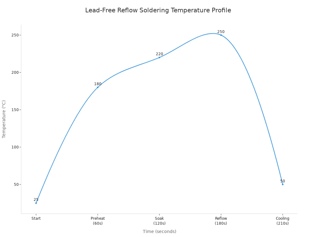
This table shows a typical temperature profile for lead-free solder.
| Zone | Parameter | Lead-Free Solder Value |
|---|---|---|
| Preheat | Temperature Rise Rate | 1.5°C to 3°C per second |
| Soak | Temperature Range | 180°C to 220°C |
| Reflow | Peak Temperature | 240°C to 250°C |
| Cooling | Cooling Rate | 2°C to 4°C per second |
How is heat applied evenly? 🤔 Modern reflow ovens use forced air convection. Fans circulate hot air to ensure every part of the PCB heats uniformly. Advanced systems like plenum or horizontal convection technology perfect this process, preventing hot or cold spots.
To improve solder quality, you can introduce nitrogen into the oven. A nitrogen atmosphere reduces oxidation. This enhances solder flow and leads to stronger, more reliable joints with fewer defects.
THT Wave Soldering
You use wave soldering for through-hole components. This bulk soldering method is highly efficient for mass production. It allows you to solder many joints at once. The process involves passing the PCB over a wave of molten solder.
The wave soldering process follows four key steps:
- Flux Application: You first apply a layer of flux to the bottom of the PCB. The flux cleans the metal surfaces and removes oxides.
- Preheating: You preheat the board to between 100°C and 150°C. This activates the flux and prevents thermal shock when the board hits the hot solder.
- Solder Wave: The PCB passes over a pan of molten solder. A pump creates a wave that touches the underside of the board, soldering all the component leads.
- Cooling: The board cools down after leaving the wave. The solder solidifies, creating strong mechanical and electrical connections.
Just like in reflow, using a nitrogen atmosphere during wave soldering offers major benefits. It prevents oxide formation on the solder wave. This improves wetting and reduces defects like bridging and incomplete solder joints.
Manual and Selective Soldering
Sometimes, a board has a mix of SMT and THT components. You cannot use wave soldering on these mixed-technology boards because it would damage the already-soldered surface mount components. This is where you need a more targeted approach.
-
Manual Soldering: A skilled technician uses a soldering iron to solder individual components by hand. This is common for prototypes, repairs, or adding sensitive components after automated processes. It offers high precision but is slow and not scalable for large volumes.
-
Selective Soldering: This is an automated process that bridges the gap between wave and manual soldering. A machine uses a tiny nozzle to apply molten solder only to specific through-hole pins.
This method is much faster than hand soldering and more precise than wave soldering for mixed-technology PCBs. It ensures high-quality joints without risking damage to the rest of the assembly.
Post-Assembly Quality Assurance
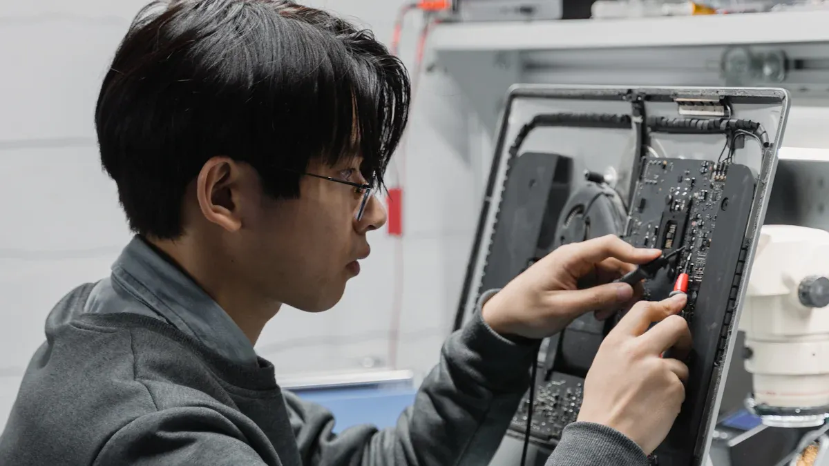
After soldering, your PCB is assembled, but you must verify its quality. This quality assurance stage ensures every connection is perfect and every component is correctly placed. You use several inspection methods to catch any potential defects.
Manual Visual Inspection
The first line of defense is a manual visual inspection. A trained technician looks at each PCB, often with a microscope. They check the solder joints against industry standards, like IPC-A-610.
A good solder joint is key to a reliable PCB. According to the IPC standard, an acceptable joint has:
- A wetting angle less than 90 degrees.
- A concave fillet, which looks like a smooth curve from the component to the board.
- Good solder coverage on the pad.
This hands-on check is great for finding obvious errors, but it can be slow and is not practical for every single board in a large production run.
Automated Optical Inspection (AOI)
You use Automated Optical Inspection (AOI) for fast and consistent checks. An AOI machine uses high-resolution cameras to take pictures of the PCB. It then compares these images to your design files to spot errors. AOI is excellent at finding:
- Missing or incorrectly placed components
- Wrong component polarity
- Solder bridges (shorts) or insufficient solder
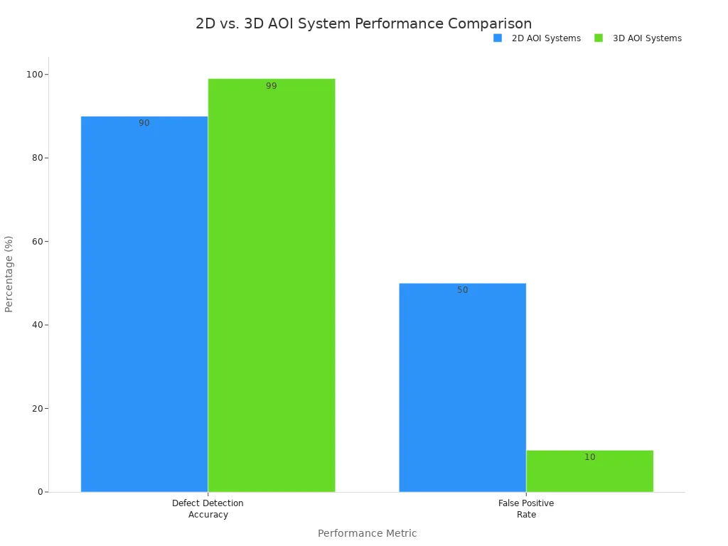
Modern systems use 2D or 3D imaging. A 3D AOI provides much more detail.
| Feature | 2D AOI Systems | 3D AOI Systems |
|---|---|---|
| Detection Method | Top-down image comparison | 3D mapping with multiple cameras |
| Key Advantage | Fast for surface defects | Measures component height and solder volume |
| Limitations | Cannot see hidden defects | Fewer limitations |
3D AOI is better at catching subtle issues, leading to a higher quality printed circuit board assembly.
X-ray Inspection (AXI)
Some components have solder joints hidden underneath them. You cannot see these with a camera. This is where you use Automated X-ray Inspection (AXI). AXI allows you to see through components to inspect the connections below. It is essential for parts like:
AXI can find hidden solder bridges, open circuits, and voids within the solder.
Final PCB Assembly Inspection
Before the PCB moves to testing, it undergoes a final inspection. This step confirms the board meets all specifications. Technicians verify component placement, check for board warpage, and ensure all previous inspection steps were passed. This final check guarantees the PCB is built correctly before you power it on for the first time.
Final Testing and Finishing
Your PCB is now assembled, but the journey isn't over. You must perform final testing and finishing to ensure it works perfectly and is protected from the environment. This is the last stage of the pcb assembly process.
In-Circuit and Functional Testing
You start with the first part of the final testing and validation: electrical testing. This confirms every part of your PCB works as designed. You use two main types of tests: In-Circuit Testing (ICT) and Functional Testing (FCT).
| Feature | In-Circuit Testing (ICT) | Functional Testing (FCT) |
|---|---|---|
| Primary Focus | Individual components | The entire board's function |
| Objective | Checks for soldering faults | Verifies product functionality |
| Method | Uses a "bed-of-nails" fixture | Simulates a real operating environment |
ICT uses a fixture with many pins, called a bed-of-nails, to check each component individually. This method is great because it:
- Finds faults very quickly.
- Achieves up to 95% test coverage on a complex PCB.
- Reduces labor costs by automating the process.
FCT, on the other hand, powers up the entire PCB to see if it performs its intended job. This test confirms the board works in the real world.
Board Cleaning and Residue Removal
After soldering, you may have leftover flux residue on the board. While some "no-clean" fluxes can be left on, cleaning the PCB is often a good idea for long-term reliability. You can remove residue in a few ways:
- Wet: Apply a solvent like isopropyl alcohol to dissolve the residue.
- Scrub: Gently use a soft brush to loosen any tough spots.
- Rinse: Wash the board with a clean solvent.
- Dry: Use forced air to dry the PCB completely.
For high-volume production, you use automated cleaning systems to handle this process efficiently.
Applying Conformal Coating
To protect your PCB from moisture, dust, and extreme temperatures, you apply a thin layer of protective material called a conformal coating. The type of coating you choose depends on the product's needs.
- Acrylic: Good for moisture protection and easy to repair.
- Silicone: Excellent for products used in very high or low temperatures.
You can apply the coating by dipping the entire board into a tank or by using an automated spray system. Spraying gives you better control over the coating thickness and is great for high-volume jobs.
Depaneling and Final Assembly
Your boards are often manufactured in a large panel containing several copies of the same PCB. Depaneling is the process of separating these individual boards from the panel. You can use several methods, from a simple V-cut blade to a high-precision laser that makes clean cuts without stressing the components.
Once the boards are separated, they are ready for final assembly. This could involve placing them into an enclosure or connecting them to other parts of a larger product. This completes the final testing and validation, and your PCB is now ready for action! 🚀
You have seen how a bare board becomes a functional PCB. The journey moves from applying solder paste and placing components to soldering and final testing. Each step is vital for a successful outcome.
Following strict industry standards, like IPC and ISO 9001, ensures every PCB meets high-quality and reliability targets.
This systematic method is the backbone of every electronic device you use. It turns simple designs into the powerful technology that shapes our world. 🚀
FAQ
What is the main difference between SMT and THT?
You place Surface Mount Technology (SMT) components directly onto the board's surface. You insert Through-Hole Technology (THT) components through drilled holes. SMT allows for smaller designs, while THT provides stronger mechanical bonds for larger parts like connectors.
Why is the Bill of Materials (BOM) so important?
Your Bill of Materials (BOM) acts as the complete parts list for your project. It ensures your manufacturer sources the exact components your design needs. An accurate BOM prevents costly errors and production delays, guaranteeing a successful assembly.
Can you use both SMT and THT on the same PCB?
Yes, you certainly can. This is called a "mixed-technology" board. Manufacturers typically assemble the SMT components first using reflow soldering. Afterward, they add the THT components using a more precise method like selective or manual soldering.
What are fiducial marks?
Fiducial marks are small, circular patterns you place on your PCB. Automated assembly machines use these marks as reference points. They allow the machine's camera to find the board's exact position, ensuring every component is placed with high accuracy. 🤖