A Beginner's Guide to PMOS and NMOS Differences
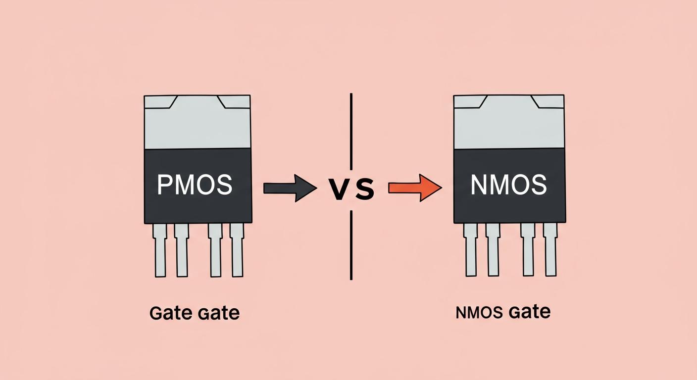
Modern digital devices contain billions of transistors. For instance, Apple's M2 Max processor has 67 billion. Many of these are a special field-effect transistor (FET). This type of MOSFET is fundamental to electronics. The two main types are the PMOS transistor and the NMOS transistor. They are both Metal-Oxide-Semiconductor Field-Effect Transistors, but they operate with opposite logic. This difference is critical for every digital application.
An NMOS switch turns ON with a HIGH signal, like pressing a button. A PMOS switch turns ON with a LOW signal, like releasing a button.
Understanding this opposing function is vital for countless digital applications. The specific application of each MOSFET depends on this behavior, defining its role in a circuit.
Key Takeaways
- NMOS and PMOS transistors are basic parts of digital devices. They work in opposite ways.
- NMOS transistors turn on with a high signal. They use electrons, which move fast. This makes NMOS good for speed.
- PMOS transistors turn on with a low signal. They use 'holes,' which move slower than electrons.
- Combining NMOS and PMOS creates CMOS circuits. These circuits use very little power and are found in almost all modern digital devices.
PMOS vs. NMOS: Core Structural Differences
The opposing behaviors of PMOS and NMOS transistors originate from their fundamental structural differences. Each transistor is built upon a base material called a substrate. The type of substrate and the materials added to it define the transistor's identity and function. The entire structure is a marvel of material science, designed to control the flow of electricity with incredible precision.
The N-Channel Structure
An N-channel Metal-Oxide-Semiconductor (NMOS) transistor has a specific layered structure. The foundation is a P-type silicon substrate, which acts as the body of the transistor. Engineers create two distinct N-type regions within this P-type body by doping them with elements like Phosphorus or Arsenic. These regions become the Source and the Drain.
A very thin insulating layer separates the gate terminal from the semiconductor body. This layer is critical for the field-effect transistor to work.
The body terminal itself is essential for proper operation. It is typically connected to a voltage lower than the source and drain. This connection ensures that no unwanted current leaks from the body into the channel. This careful construction defines the n-channel MOSFET structure.
The P-Channel Structure
A P-channel Metal-Oxide-Semiconductor (PMOS) transistor is the structural opposite of an NMOS transistor. A PMOS device uses an N-type silicon substrate as its foundation. Within this N-type body, engineers form two P-type regions that serve as the Source and Drain. This inverted structure is the key to its unique function.
Like the NMOS transistor, a PMOS transistor also has a gate terminal made of polysilicon. This gate is insulated from the N-type body by a thin layer of silicon dioxide. The materials are the same, but their arrangement is reversed. This p-channel MOSFET structure is designed to respond to different electrical conditions than its N-channel counterpart.
Charge Carriers: Electrons vs. Holes
The most important consequence of the different structures is the type of charge carrier each transistor uses. This directly impacts their performance.
- NMOS: In an n-channel metal-oxide-semiconductor device, the charge carriers are electrons. Electrons are negatively charged particles that move freely through the semiconductor material.
- PMOS: In a p-channel metal-oxide-semiconductor device, the charge carriers are electron holes.
This difference in charge carriers is not just academic; it has a major impact on speed. Electrons move much more easily through silicon than holes do.
| Carrier | Mobility (cm²/V·s) |
|---|---|
| Electrons | ≤1400 |
| Holes | ≤450 |
As the table shows, the mobility of electrons is significantly higher than that of holes. This means an NMOS transistor can switch on and off much faster than a PMOS transistor of the same size, a crucial factor in designing high-speed circuits.
How Each Transistor Operates
The physical structure of a transistor directly controls its electrical behavior. The gate terminal acts as the master control for all switching operations. Applying a specific voltage to the gate determines whether the transistor is ON (allowing current to flow) or OFF (blocking current). This simple on/off capability is the foundation of all digital logic.
NMOS Transistor Activation
An NMOS transistor requires a positive voltage to turn on. The key to its operation is a value called the threshold voltage (Vth). The threshold voltage is the minimum gate-to-source voltage (VGS) needed to create a conducting path between the source and drain. This voltage level marks the critical point for the transistor's switching action.
When the gate voltage is higher than the threshold voltage, the transistor activates.
- A positive voltage on the gate creates an electric field across the oxide layer.
- This field pushes the positive holes away from the area under the gate.
- Simultaneously, the field attracts negative electrons from the P-type substrate.
- These electrons gather at the surface, forming a thin "inversion layer" or channel.
This newly formed channel provides a conductive bridge between the N-type source and drain. Current can now flow freely, turning the n-channel metal-oxide-semiconductor transistor ON. If the gate voltage is below the threshold voltage, the n-channel MOSFET remains in its "cut-off" state. No channel forms, and the device acts like an open switch, blocking current flow.
Threshold Voltage: The Switching Point A MOSFET transitions from the cutoff region (OFF) to the active region (ON) only when the gate voltage surpasses its threshold voltage. Below this point, no significant current flows. This precise control makes the MOSFET an excellent component for digital switching.
PMOS Transistor Activation
A PMOS transistor operates in the exact opposite manner. It requires a low voltage (or a voltage that is negative relative to its source) to turn on. The charge carriers in a p-channel metal-oxide-semiconductor device are holes, not electrons. The goal of activation is to form a channel of these positive holes.
The activation process for a PMOS transistor involves these steps:
- A low voltage is applied to the gate terminal.
- This creates an electric field that repels the free electrons in the N-type substrate.
- The field attracts positive holes from the P-type source and drain regions to the area under the gate.
- When enough holes accumulate, they form a P-type conductive channel.
This channel allows current to flow from the source to the drain, turning the p-channel MOSFET ON. If the gate voltage is high, no channel forms, and the PMOS transistor remains OFF. This complementary behavior is essential for creating efficient circuits. The switching mechanism of this transistor is fundamental to its role in electronics.
Simple On/Off State Logic
In digital electronics, we represent information using binary code: '1's and '0's. These logic levels correspond to high and low voltages. The on/off states of NMOS and PMOS transistors map directly to this binary system, making them perfect for building logic gates.
- Logic '1' = High Voltage
- Logic '0' = Low Voltage
The way each transistor responds to these logic levels is completely opposite, which is their greatest strength when used together. An NMOS transistor is excellent at passing a strong logic '0', while a PMOS transistor excels at passing a strong logic '1'.
The following table summarizes the switching logic for each transistor type:
| Transistor Type | Gate Voltage | Binary Logic | State | Current Flow |
|---|---|---|---|---|
| NMOS | High | 1 | ON | ✅ Yes |
| NMOS | Low | 0 | OFF | ❌ No |
| PMOS | Low | 0 | ON | ✅ Yes |
| PMOS | High | 1 | OFF | ❌ No |
This table clearly shows that a logic '1' turns an NMOS on but turns a PMOS off. Conversely, a logic '0' turns a PMOS on but turns an NMOS off. This opposing but predictable switching behavior is the key to modern low-power circuit design.
Performance, Speed, and Density
The structural differences between PMOS and NMOS transistors lead to major distinctions in performance. These differences in speed, power, and size determine where each transistor is used. For designers of modern electronics, understanding these trade-offs is essential for creating efficient and powerful devices.
The Electron Mobility Advantage
The primary performance difference comes from their charge carriers. An NMOS transistor uses electrons, while a PMOS transistor uses holes. Electrons move through the semiconductor material much more easily than holes. This gives the NMOS transistor a significant advantage.
Think of electrons as cars on a superhighway and holes as cars on a crowded city street. The electrons can travel much faster. Because of this higher mobility, an NMOS transistor has lower resistance than a PMOS transistor of the same physical size. This lower resistance is a key factor in its superior performance.
Impact on Switching Speed
A transistor's main job in digital logic is switching on and off very quickly. The switching speed depends on how fast the transistor can charge and discharge its internal capacitances. A faster charge/discharge cycle results in a faster switching speed.
The Rule of Speed: Faster charging and discharging of the gate equals a faster switching speed. ⚡
The lower resistance of an NMOS transistor allows more current to flow. This higher current enables the transistor to charge and discharge its gate much faster than a PMOS device. This faster switching capability makes the n-channel mosfet the preferred choice for building high-speed digital circuits. The superior switching speed of NMOS is critical for the performance of modern processors. This is a fundamental principle of fast switching.
Transistor Size and Density
The efficiency of an NMOS transistor has another major benefit: size. Since an NMOS device is more efficient at conducting current, it can be made physically smaller than a PMOS transistor while still providing the same electrical performance. This size difference has a huge impact on chip design.
Smaller transistors allow engineers to pack more of them onto a single semiconductor chip. This concept is the foundation of Moore's Law. Increasing transistor density leads to several key benefits:
- More Power: More transistors mean more computational capability.
- Higher Speed: Shorter distances between components improve overall switching speed.
- Lower Cost: Manufacturing more transistors on one wafer reduces the cost per transistor.
This ability to create smaller, faster components is why NMOS technology dominates the world of high-performance computing. The constant drive for faster switching and greater density continues to push technology forward.
Circuit Roles and the CMOS MOSFET
The opposite behaviors of PMOS and NMOS transistors make them perfect partners in digital circuits. Designers assign each transistor a specific job. One pulls the circuit's output high, and the other pulls it low. This teamwork is the basis for modern electronics.
The Pull-Down Network
An NMOS transistor is ideally suited for creating a pull-down network. This network's job is to connect a circuit's output to Ground (0V). An NMOS transistor turns on when its gate receives a high voltage (a logic '1'). When this switch is on, it creates a low-resistance path between the output and Ground. This action effectively pulls the output voltage down to a logic '0'. This characteristic is fundamental for the pull-down network in digital logic circuits. The NMOS transistor acts as a gatekeeper to the ground connection.
The Pull-Up Network
A PMOS transistor performs the opposite role in a pull-up network. This network connects the circuit's output to the power supply (VDD). A PMOS transistor turns on when its gate voltage is low (a logic '0'). This activation creates a path for current to flow from the power supply to the output. The p-channel mosfet is excellent at passing a strong logic '1' signal. This ensures the output reaches the full supply voltage. This reliable switching makes the PMOS transistor the perfect choice for pulling an output high.
The CMOS Advantage
Combining a PMOS pull-up network with an NMOS pull-down network creates a complementary metal-oxide semiconductor, or CMOS, circuit. This design is the foundation of almost all modern digital devices. The key benefit of CMOS technology is its incredible efficiency.
In a CMOS configuration, only one transistor (either the PMOS or the NMOS) is on at any given time during a steady state. This prevents a direct path from power to ground, resulting in very low static power consumption.
This complementary logic gates structure provides several major benefits:
- Low Power Use: Minimal power is consumed when the circuit is not actively switching.
- High Noise Immunity: CMOS circuits have a wide noise margin. This makes them very resistant to electrical interference.
- Reliable Switching: The PMOS and NMOS transistors ensure the output is always strongly pulled to either high or low.
Because of these advantages, complementary metal-oxide semiconductor technology became the standard for manufacturing integrated circuits. Today, 99% of semiconductor chips, including microprocessors, memory chips, and microcontrollers, use CMOS for their digital applications. This powerful pairing of the PMOS and NMOS mosfet enables our complex digital world.
PMOS and NMOS transistors are the essential building blocks of our digital world. The NMOS transistor is a fast workhorse for pull-down logic, while the PMOS transistor is its perfect partner for pull-up logic. Their combination creates complementary metal-oxide semiconductor (CMOS) technology. This CMOS pairing is the key to efficient, low-power digital electronics.
A basic CMOS inverter, the foundation of digital logic gates, shows how they work together.
- The input connects to the gates of both the PMOS and NMOS transistor.
- The PMOS transistor source connects to the power supply.
- The NMOS transistor source connects to the ground.
- The output is taken from the connected drains of each transistor.
This complementary metal-oxide semiconductor design ensures low power use. Understanding this PMOS and NMOS partnership in CMOS is the first step toward mastering digital logic.
FAQ
Why is NMOS faster than PMOS?
NMOS transistors use electrons to carry charge. Electrons move through silicon about 2.5 times faster than the holes used by PMOS transistors. This superior electron mobility results in significantly faster switching speeds for NMOS devices, making them ideal for high-performance logic.
Why do circuits use both PMOS and NMOS?
Designers use both transistors for maximum efficiency. A PMOS transistor excels at pulling an output to a high voltage ('1'). An NMOS transistor is perfect for pulling an output to a low voltage ('0'). This complementary pairing creates low-power CMOS circuits.
What does CMOS stand for?
CMOS stands for Complementary Metal-Oxide-Semiconductor.
The term "Complementary" highlights the design's core principle. It uses both PMOS (pull-up) and NMOS (pull-down) transistors working together as a perfect pair in a single logic gate. This teamwork is the key to its efficiency. 💡
Can you build a circuit with only NMOS transistors?
Yes, circuits can use only NMOS transistors. This approach, called NMOS logic, was common in early microprocessors. However, these designs consume much more power than modern CMOS circuits. The superior efficiency of CMOS technology eventually made it the dominant industry standard.