The Impact of NMOS and PMOS Differences on Integrated Circuit Design
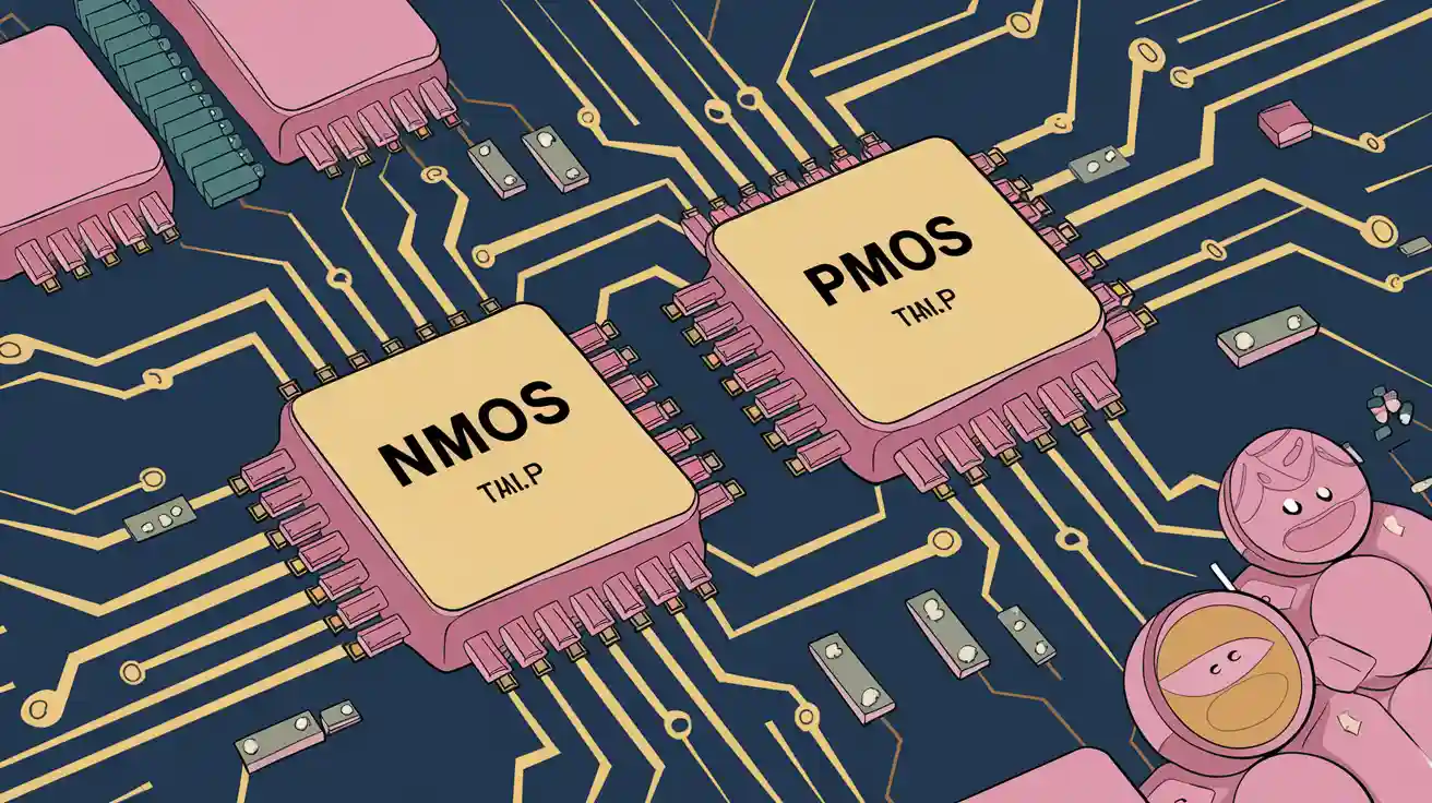
The nmos vs pmos debate shapes how engineers approach transistor selection in integrated circuits. NMOS transistors, which use electrons as charge carriers, offer higher mobility than PMOS transistors that rely on holes. This difference means NMOS transistors switch faster and deliver greater drive current, directly impacting speed and power efficiency. For example, hybrid designs that combine high-mobility NMOS with PMOS can reduce rise time and propagation delay by over 70%. Understanding these characteristics helps designers choose the right transistor for each circuit, ensuring optimal performance in modern design.
Key Takeaways
NMOS transistors switch faster and use less space, making them ideal for high-speed digital circuits and dense layouts.
PMOS transistors offer better power efficiency and noise immunity, which suits low-power and sensitive analog applications.
Combining NMOS and PMOS in CMOS technology balances speed and power use, creating reliable and energy-efficient circuits.
Designers choose transistor types based on speed, power needs, and circuit roles to optimize performance and stability.
Understanding NMOS and PMOS differences helps engineers build faster, smaller, and more efficient integrated circuits.
NMOS vs PMOS: Definitions
NMOS Overview
An n-channel metal-oxide-semiconductor, or NMOS, is a type of metal-oxide-semiconductor field-effect transistor. Engineers use NMOS transistors widely in digital circuits because they offer fast switching and high drive current. The NMOS structure includes n-type doped source and drain regions on a p-type silicon substrate. When a positive voltage is applied to the gate, the NMOS transistor forms a conductive channel, allowing electrons to flow from source to drain. This electron flow gives NMOS devices higher mobility and faster operation compared to PMOS. NMOS transistors are often smaller for the same output current, which helps increase layout density in integrated circuits. In the nmos vs pmos comparison, NMOS devices typically serve as the pull-down network in CMOS logic, pulling the output to ground.
NMOS transistors conduct when the gate-to-source voltage is positive. They are normally off and require a positive voltage to turn on. This property makes them ideal for low-side switching and high-speed digital logic.
Aspect | NMOS Transistor |
|---|---|
N-type doped source and drain; P-type substrate | |
Majority Charge Carrier | Electrons |
Gate-to-Source Voltage | Positive VGS required to form channel |
Faster | |
Typical Usage | Low-side switching, digital logic |
PMOS Overview
A p-channel metal-oxide-semiconductor, or PMOS, is another type of field-effect transistor. PMOS transistors use p-type doped source and drain regions on an n-type silicon substrate. When a negative voltage is applied to the gate, the PMOS transistor forms a conductive channel, allowing holes to flow from source to drain. This hole conduction results in lower mobility and slower switching compared to NMOS. PMOS transistors are valued for their power efficiency and noise immunity, making them suitable for high-side switching and noise-sensitive applications. In CMOS technology, PMOS devices complement NMOS by pulling the output to the supply voltage.
PMOS transistors conduct when the gate-to-source voltage is negative.
They are normally on in some configurations but usually operate in enhancement mode.
PMOS devices have higher on-resistance and require a larger area for the same current as NMOS.
Aspect | PMOS Transistor |
|---|---|
Physical Construction | P-type doped source and drain; N-type substrate |
Majority Charge Carrier | Holes |
Gate-to-Source Voltage | Negative VGS required to form channel |
Conduction Speed | Slower |
Typical Usage | High-side switching, noise-sensitive circuits |
The difference between pmos and nmos lies in their charge carriers, switching behavior, and roles in semiconductor circuits. Both types of MOSFETs are essential for modern integrated circuit design, especially in CMOS technology, where their complementary action enables efficient logic operations.
Difference Between PMOS and NMOS: Core Characteristics
Charge Carriers and Mobility
The difference between pmos and nmos begins with their charge carriers. An n-channel metal-oxide-semiconductor, or NMOS, uses electrons as the main carriers. These electrons move quickly through the semiconductor, giving NMOS transistors higher mobility. In contrast, a p-channel metal-oxide-semiconductor, or PMOS, relies on holes, which are slower and have lower mobility. This core distinction affects how fast each transistor can switch and how much current it can drive.
Characteristic | NMOS Transistor | PMOS Transistor |
|---|---|---|
Electrons (negatively charged) | Holes (positively charged) | |
Carrier Mobility | Higher mobility | Lower mobility |
Drive Current | Higher due to higher mobility | Lower due to lower mobility |
Faster | Slower | |
On-Resistance | Lower | Higher |
Engineers often choose NMOS for speed-critical paths in integrated circuits. PMOS, with its lower mobility, finds use in roles where power efficiency and noise immunity matter more.
Structural Differences
NMOS and PMOS transistors differ in their internal structure. NMOS devices have n-type source and drain regions on a p-type substrate. PMOS transistors use p-type source and drain regions on an n-type substrate. This difference in doping changes how each field-effect transistor operates.
Feature | NMOS Transistor | PMOS Transistor |
|---|---|---|
N-type source/drain, p-type substrate | P-type source/drain, n-type substrate | |
Size and Density | Smaller, higher packing density | Larger, lower packing density |
Power Consumption | Higher static power | Lower static power |
Noise Immunity | Lower | Higher |
Applications | High-speed digital, memory | Analog, power management, low-power digital |
The comparison between nmos and pmos shows that NMOS transistors, with their smaller size and faster switching, suit high-speed digital circuits. PMOS transistors, with better noise immunity, often appear in analog and power management applications.
Gate Voltage Polarity
Gate voltage polarity sets NMOS and PMOS apart in circuit design. NMOS transistors turn on when the gate voltage is positive compared to the source. PMOS transistors require a negative gate voltage relative to the source to conduct. This difference between pmos and nmos affects how engineers connect them in integrated circuits.
NMOS: Turns on with positive gate-to-source voltage.
PMOS: Turns on with negative gate-to-source voltage.
The source terminal is at the lower voltage for NMOS and at the higher voltage for PMOS.
This polarity difference plays a key role in how designers use each type of metal-oxide-semiconductor field-effect transistor in logic gates, switches, and power management circuits. Understanding these core characteristics helps engineers select the right transistor for each semiconductor application.
NMOS vs PMOS: Electrical Performance
Switching Speed
Switching speed stands out as a key technical advantage in the comparison between nmos and pmos transistors. NMOS transistors switch faster than PMOS because electrons move more quickly than holes. This higher electron mobility gives NMOS a lower on-resistance and better channel conductivity. Engineers often choose NMOS for high-speed digital circuits and microprocessors. PMOS transistors, with slower hole movement, switch at a lower speed. However, PMOS provides better noise immunity, which helps in sensitive analog circuits.
NMOS switches faster due to higher electron mobility.
PMOS offers slower switching but better noise performance.
CMOS technology combines both to balance speed and efficiency.
Power Consumption
Power consumption is another important technical advantage when comparing these two types of MOSFET transistors. NMOS transistors draw more current and use more power, especially during switching. PMOS transistors, on the other hand, require less energy to move holes, leading to lower power consumption. This makes PMOS ideal for battery-powered and energy-sensitive devices. The table below shows a performance comparison of power use in different applications:
Aspect | PMOS Transistors | NMOS Transistors |
|---|---|---|
Power Consumption | Lower power consumption, only during switching; lower leakage currents | Higher power consumption due to continuous current flow when on |
Application Focus | Preferred in low-power integrated circuits for energy efficiency | Favored in high-performance circuits for speed despite higher power use |
Performance | Slower switching speed, better noise immunity | Faster switching speed, suitable for rapid data processing |
Designers often use both NMOS and PMOS in CMOS circuits to balance power and performance.
Threshold Voltage
Threshold voltage defines when a transistor turns on. NMOS transistors conduct when the gate voltage rises above the source voltage. PMOS transistors conduct when the gate voltage drops below the source voltage. This difference affects how engineers design logic gates and switches. NMOS usually needs a positive gate voltage, while PMOS needs a negative one. These characteristics help engineers select the right transistor for each part of an integrated circuit.
Tip: Understanding threshold voltage helps engineers avoid unwanted switching and improve circuit reliability.
The nmos vs pmos discussion highlights how these electrical properties shape the technical advantages of each transistor type. By combining NMOS and PMOS in CMOS technology, designers achieve efficient, high-performance circuits for many applications.
Impact on Circuit Design
Speed-Critical Paths
Engineers often face challenges when selecting transistors for speed-critical paths in circuit design. NMOS transistors offer higher electron mobility, which leads to faster switching speeds and better conductivity. These technical advantages make NMOS ideal for high-speed digital circuits. Designers place NMOS transistors in pull-down paths to achieve quick response times. PMOS transistors, with lower hole mobility, switch slower and have higher resistance. This disadvantage limits their use in speed-sensitive areas. PMOS transistors usually appear in pull-up paths, where power efficiency and noise immunity matter more than speed. The complementary use of NMOS and PMOS in CMOS technology balances speed and power efficiency. PMOS transistors require careful timing and layout optimization because of their higher threshold voltage and slower switching.
Feature | NMOS Transistor Characteristics | PMOS Transistor Characteristics |
|---|---|---|
Charge Carrier Mobility | Higher electron mobility leading to faster switching | Lower hole mobility causing slower switching |
Switching Speed | Faster switching speeds ideal for speed-critical paths | Slower switching speeds limiting use in high-speed paths |
Circuit Role | Commonly used in low-side (pull-down) paths for speed | Used in high-side (pull-up) paths where speed is less critical |
Threshold Voltage | Lower threshold voltage facilitating quicker turn-on | Higher threshold voltage requiring more voltage to activate |
Conductivity | Better conductivity supporting faster response times | Higher resistance reducing speed performance |
Layout Density
Layout density plays a key role in modern integrated circuits. NMOS transistors have a smaller size for the same output current, which allows engineers to pack more devices into a given area. This technical advantage leads to higher integration density and supports complex circuit design. PMOS transistors, on the other hand, require a larger area because of their lower mobility and higher on-resistance. This disadvantage reduces layout density and can increase manufacturing costs. Designers often use NMOS transistors in speed-critical and space-constrained applications. PMOS transistors appear in complementary configurations, such as CMOS, where their larger size is offset by the benefits of low power consumption and improved noise immunity.
Tip: Maximizing layout density with NMOS transistors helps engineers create smaller, faster, and more efficient integrated circuits.
Signal Integrity
Signal integrity determines how well a circuit maintains clean and reliable signals. NMOS transistors switch quickly, which suits high-speed operations but can lead to lower noise margins and higher energy consumption. This disadvantage makes NMOS more susceptible to electrical noise. PMOS transistors switch slower but provide better noise immunity, lower leakage current, and higher voltage stability. These technical advantages make PMOS valuable in noise-sensitive applications. When engineers combine NMOS and PMOS in CMOS technology, they improve signal integrity and noise margins. NMOS provides fast switching, while PMOS adds stability and noise resistance. This synergy reduces power consumption and enhances reliability in high-speed integrated circuits.
Characteristic | NMOS Transistors | PMOS Transistors |
|---|---|---|
Charge Carrier Mobility | High electron mobility, enabling faster switching | Lower hole mobility, resulting in slower switching |
Switching Speed | Faster, ideal for high-speed digital circuits | Slower, limits high-speed signal processing |
Energy Consumption | Higher power consumption in ON state | Lower leakage current, better for low-power devices |
Noise Margin & Immunity | Lower noise margin, more susceptible to noise | Better noise immunity, generates less switching noise |
Voltage Stability | Less stable under high voltage | More stable and reliable in high voltage environments |
Size and Density | Smaller size, supports higher integration density | Generally larger than NMOS for same function |
Role in CMOS Technology | Provides strong '0' signal and fast switching | Provides strong '1' signal and stability |
CMOS technology combines NMOS and PMOS transistors to leverage their individual strengths.
NMOS transistors provide fast switching speeds due to high electron mobility.
PMOS transistors offer low power consumption and high noise immunity because of low leakage currents and robustness at high voltages.
In CMOS circuits, NMOS acts as a pull-down device connecting output to ground when active.
PMOS acts as a pull-up device connecting output to the supply voltage (Vdd) when active.
This complementary action results in power consumption mainly during switching, drastically reducing static power dissipation compared to circuits using only NMOS or PMOS.
CMOS circuits thus enable energy-saving, high-speed, and efficient digital integrated circuits suitable for battery-powered devices and large-scale integration.
The complementary use also ensures stable logic levels and reduces power loss, enhancing overall device reliability and performance.
The nmos vs pmos comparison shows that each transistor type brings unique advantages and disadvantages to circuit design. NMOS transistors excel in speed and layout density, while PMOS transistors provide better noise immunity and power efficiency. Engineers achieve optimal performance by combining both in CMOS technology, which improves signal integrity and supports reliable operation in integrated circuits.
Application Scenarios for NMOS, PMOS, and CMOS
NMOS Applications
Engineers often select nmos transistors for high-speed digital circuits. These devices excel in microprocessors, memory cells, and integrated circuits that demand fast switching. The main advantages of nmos include higher electron mobility and lower on-resistance, which support rapid data processing. Designers use nmos in cost-effective digital electronics where speed is a priority. However, disadvantages such as higher static power consumption and lower noise immunity can limit their use in low-power digital circuits. In semiconductor manufacturing, nmos technology remains a popular choice for applications that require quick response times and compact layouts.
PMOS Applications
Pmos transistors serve important roles in circuits that need voltage stability and low leakage current. Engineers use pmos in analog amplifiers, voltage level shifters, and power management circuits. These devices offer advantages like better noise immunity and reliable operation in power-sensitive applications. Pmos technology helps protect against overvoltage and supports voltage level shifting in mixed-signal semiconductor systems. Disadvantages include slower switching speeds and larger device size compared to nmos. Despite these drawbacks, pmos remains valuable in applications where energy efficiency and signal integrity matter most.
CMOS Technology
Cmos technology, which stands for complementary metal oxide semiconductor, combines nmos and pmos transistors in complementary logic gates. This approach brings together the advantages of both types, resulting in low static power consumption and high noise immunity. Cmos dominates modern digital logic circuits, including microprocessors, memory chips, and logic circuits. Its use extends across consumer electronics, automotive systems, medical devices, aerospace, and industrial automation. Cmos enables energy-efficient, miniaturized, and scalable semiconductor devices. While cmos fabrication is more complex and costly, its advantages in power efficiency and scalability outweigh the disadvantages for most applications. The integration of nmos and pmos in cmos supports the development of reliable, high-performance digital systems.
Technology | Common Application Scenarios | Key Consumer & Industrial Uses |
|---|---|---|
NMOS | High-speed digital circuits, microprocessors, memory cells, integrated circuits | Used for fast switching and cost-effective digital electronics |
PMOS | Low-power digital circuits, analog amplifiers, voltage level shifters, power management circuits | Preferred for lower leakage current and voltage stability in power-sensitive applications |
CMOS | Combines NMOS and PMOS; digital electronics like microprocessors, memory chips, logic circuits | Widely used in consumer electronics, automotive, medical, aerospace, and industrial automation |
Tip: Choosing between nmos, pmos, and cmos depends on the specific performance needs, such as speed, power consumption, and scalability, for each semiconductor application.
Practical Design Considerations
Design Constraints
Engineers must consider several constraints when selecting NMOS or PMOS transistors for a circuit. Each type offers unique advantages and disadvantages that affect performance and application. The table below highlights key factors:
Design Constraint | NMOS Transistors | PMOS Transistors |
|---|---|---|
Switching Speed | Faster switching due to higher electron mobility | Slower switching due to lower hole mobility |
Power Consumption | Higher power consumption, especially when on | Lower power consumption and leakage current |
Noise Immunity | Lower noise immunity | Higher noise immunity |
Voltage Stability | Less robust at high voltages | More robust at high voltages |
Physical Size | Smaller physical size | Larger physical size, challenging miniaturization |
Cost | More cost-effective | Generally more expensive |
Typical Applications | High-speed digital circuits, microprocessors, memory cells | Low-power digital circuits, analog amplifiers, voltage level shifters, power management circuits |
NMOS transistors provide advantages in speed and cost, making them suitable for high-speed digital circuits. PMOS transistors offer advantages in noise immunity and voltage stability, which are important for sensitive applications. Designers often use both types in CMOS technology to balance these constraints.
Manufacturing Factors
Manufacturing processes introduce variability in transistor performance. Differences in doping, layer thickness, and lithography can cause changes in threshold voltage and transconductance. These changes affect how a circuit operates over time. Process variation may lead to some transistors switching slower or leaking more current. As devices age, effects like Bias Temperature Instability and Hot Carrier Degradation further shift parameters. Engineers use simulation tools to predict these changes and optimize transistor sizing. This approach helps maintain the advantages of each transistor type while reducing disadvantages in the final circuit.
Reliability
Long-term reliability remains a major concern in integrated circuit operation. Both NMOS and PMOS transistors face specific challenges:
NMOS transistors mainly suffer from Positive Bias Temperature Instability, which shifts threshold voltage.
PMOS transistors experience Negative Bias Temperature Instability, causing mobility loss and increased delay.
Hot Carrier Degradation affects both types, leading to slower operation and higher leakage.
Off-State Degradation can cause functional aging and possible circuit failure.
Other reliability issues include oxide wear out, lithographic errors, and environmental stress from high temperature or voltage. These factors can reduce the advantages of fast switching or low power and introduce disadvantages such as increased leakage or device failure. Engineers must address these risks to ensure circuits remain stable and efficient throughout their lifetime.
Summary: Key Impacts of NMOS vs PMOS
Designers must understand the core differences between NMOS and PMOS to optimize integrated circuits. The following table summarizes how each transistor type operates in different regions and how this affects circuit behavior:
Region | Input Voltage (Vin) | Output Voltage (Vout) | NMOS Operating Region | PMOS Operating Region |
|---|---|---|---|---|
A | Less than NMOS threshold (VTO,n) | High (VOH) | Cutoff | Linear |
B | Low Input Level (VIL) | High (≈ VOH) | Saturation | Linear |
C | Threshold Voltage (Vth) | Around Vth | Saturation | Saturation |
D | High Input Level (VIH) | Low (≈ VOL) | Linear | Saturation |
E | Greater than (VDD + PMOS threshold VTO,p) | Low (VOL) | Linear | Cutoff |
Note: This table helps engineers predict how NMOS and PMOS will behave in different logic states, which is essential for reliable circuit design.
Key impacts on integrated circuits include:
Single polysilicon input lines and active shapes for both NMOS and PMOS allow compact layouts, supporting high-density designs.
Power bussing and output wiring run horizontally, making connections efficient and reducing design complexity.
Pull-down networks use NMOS for fast OR and AND logic, while pull-up networks use PMOS in complementary ways, affecting logic gate structure.
CMOS technology combines NMOS and PMOS to achieve both high speed and low power, making it the standard for most modern applications.
A performance comparison shows that NMOS transistors switch faster and use less area, which benefits speed-critical and dense designs. PMOS transistors offer better noise immunity and lower leakage, making them suitable for stable, low-power circuits. CMOS leverages both strengths, enabling energy-efficient and high-performance integrated circuits.
Designers often optimize at several levels, including logic, architecture, and physical layout. They use advanced materials and configurations to further improve performance and reduce power. Techniques like power gating and multi-threshold CMOS help control leakage and standby power.
Industry experts highlight several ways NMOS and PMOS differences shape integrated circuit design:
NMOS transistors deliver faster switching and lower costs, ideal for high-speed digital circuits.
PMOS transistors offer lower leakage and better voltage stability, making them suitable for low-power and analog applications.
Engineers select transistor types based on speed, power, and circuit needs.
CMOS technology combines both, balancing performance and efficiency for modern devices.
Understanding these differences helps designers create reliable, efficient circuits and encourages further exploration of CMOS for advanced projects.
FAQ
What makes NMOS transistors faster than PMOS transistors?
NMOS transistors use electrons as charge carriers. Electrons move faster than holes, which PMOS transistors use. This higher mobility allows NMOS devices to switch more quickly in digital circuits.
Why do designers combine NMOS and PMOS in CMOS technology?
Designers use both NMOS and PMOS in CMOS to balance speed and power efficiency. NMOS provides fast switching. PMOS reduces power loss. Together, they create reliable and energy-efficient integrated circuits.
Which applications benefit most from PMOS transistors?
PMOS transistors work best in circuits that need low power and strong noise immunity. Engineers use PMOS in analog amplifiers, voltage level shifters, and power management systems.
How does layout density differ between NMOS and PMOS?
Transistor Type | Layout Density | Typical Use |
|---|---|---|
NMOS | Higher | Speed-critical paths |
PMOS | Lower | Power-sensitive |
NMOS transistors require less space, allowing more devices in a chip. PMOS transistors need larger areas.
What reliability issues affect NMOS and PMOS transistors?
NMOS faces positive bias temperature instability.
PMOS experiences negative bias temperature instability.
Both types can suffer from hot carrier degradation and off-state aging.
Engineers address these issues to maintain circuit stability over time.