How to Start Designing ASIC Chips A Simple Guide
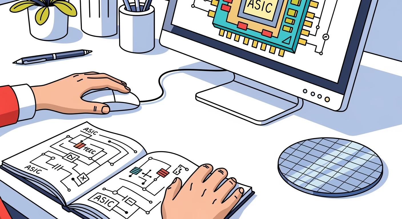
This guide provides a clear, four-step roadmap for your asic design journey. You can begin learning chip design by following these core steps:
Build Foundational Knowledge
Learn Essential Tools
Understand the Design Process
Gain Practical Experience
An ASIC is a custom microchip created for one specific job. With the global asic chip market projected to grow at 8.94% annually, learning chip design is a valuable skill. This structured path makes the asic design process achievable.
Key Takeaways
Start your ASIC design journey by learning basic chip design and digital electronics.
Learn essential tools like Hardware Description Languages (HDLs) such as Verilog and Electronic Design Automation (EDA) software.
Understand the ASIC design process, from defining specifications to physical design.
Gain practical experience by practicing with FPGAs and working on simple projects like a traffic light controller.
Build Your Foundational Knowledge
Every great journey starts with a single step. For ASIC design, that first step is building a solid foundation. You must understand the core principles before you can create a complex microchip. This section guides you through the essential knowledge for your chip design career.
The Basics of Chip Design
Chip design primarily falls into two categories: analog and digital. Analog design works with continuous signals, like sound waves. Digital chip design, the focus of this guide, uses discrete binary signals—the 1s and 0s that power computers. Digital circuits are more resistant to noise and are easier to scale with new technologies, making them ideal for complex logic.
Today, custom ASIC design is driving innovation. Tech giants use ASICs to accelerate AI tasks and reduce cloud computing costs. For example, Broadcom's AI business, which focuses on ASIC design, earned US$3.7 billion from these custom chips.
Master Digital Electronics
You need to master digital electronics to succeed in chip design. This field is the bedrock of every modern processor and memory chip. You should start by learning these fundamental concepts:
Binary Numbers: The base-2 number system that computers use.
Boolean Algebra: The mathematics behind logical operations.
Logic Gates: The basic building blocks, such as AND, OR, and NOT gates, that perform simple logic.
These elements combine to create everything from simple calculators to powerful processors. Understanding how they work is non-negotiable for chip design.
Understand Computer Architecture
Computer architecture gives you the blueprint for organizing a chip. It defines the high-level structure, including the main functional blocks and how they interact. This is a critical part of the ASIC design process. You will decide how to partition a large system into smaller, manageable parts, such as control paths and data paths. For instance, an image processing chip for a drone requires blocks for sensor input, filtering, and compression. Your architectural choices directly impact the chip's performance, power consumption, and size. This knowledge is your next step in learning more about chip design.
Learn Essential Tools and Languages
With your foundational knowledge in place, you are ready to learn the tools of the trade. Professional chip design relies on specialized software and programming languages. This step is crucial for turning your ideas into a functional circuit.
Learn Hardware Description Languages (HDLs)
You describe digital circuits using a Hardware Description Language (HDL). An HDL is not like a typical programming language. It describes hardware behavior and structure. The two main HDLs in the industry are Verilog and VHDL.
Verilog: This language is the industry standard for asic design. Its syntax is similar to the C programming language, making it concise.
VHDL: This is a powerful alternative to Verilog. Its syntax is more verbose and structured, similar to the Ada language.
SystemVerilog: This is an extension of Verilog. It adds advanced features for complex system design and verification.
Most beginners find Verilog easier to learn due to its compact style. Your choice of HDL will guide your entire chip design workflow.
Explore EDA Tools
Electronic Design Automation (EDA) tools help you design and verify your chip. You will use different tools for each stage of the asic design process. Key tool categories include:
Simulators: These tools verify your HDL code. They check if your design works as expected before you build it. Industry-standard simulators include Synopsys VCS and Siemens QuestaSim.
Synthesis Tools: These tools convert your HDL code into a list of logic gates.
Place and Route Tools: These tools physically arrange the logic gates on the silicon wafer.
Major companies like Synopsys, Cadence, and Siemens provide these powerful software suites. While professional licenses are expensive, many vendors and third-party platforms offer affordable plans for students and hobbyists. This makes learning chip design more accessible than ever.
Tip: Some cloud-based EDA platforms offer plans for individuals and small teams. This can be a great starting point for your learning journey.
Plan
Cost (Annual Billing)
Target User
Individual Premium
Individuals
Enterprise Premium
$39.9/month/member
Small companies
Master the ASIC Design Process
You are now ready to dive into the core of chip design. The asic design process is a structured workflow that takes your concept from an idea to a final blueprint. Mastering this design flow is essential for creating a functional asic chip. This journey involves several distinct stages, each building upon the last.
Define Chip Specifications
Your first step in the design process is to define the chip's specifications. You must create a detailed document that outlines exactly what your microchip will do. This includes its functions, performance targets, and power limits.
Be precise and measurable. Instead of writing 'low power,' specify a target like 'consumes less than 50 milliwatts.' Vague language leads to problems later in the chip design.
Your specification document acts as the definitive guide for the entire project. It ensures everyone on the team understands the goals of the asic design.
Write RTL Code
Next, you will write Register-Transfer Level (RTL) code. You use a Hardware Description Language (HDL) like Verilog to describe the chip's behavior. This code is a high-level abstraction of the digital circuit. Good coding practices are vital for a successful chip design.
Avoid non-synthesizable code, such as initial statements, which work in simulation but not in an asic chip.
Keep your code modular to make it easier to read and debug.
This stage of the design flow translates your written specifications into a functional description.
Perform Functional Verification
After writing your RTL code, you must verify it. Functional verification is a critical part of the asic design flow that checks if your design behaves as expected. This step often consumes up to 70% of the entire project timeline. You will write testbenches to simulate inputs and check if the outputs match your specifications. Methodologies like the Universal Verification Methodology (UVM) help you create reusable and scalable testing environments for complex chip design projects.
Run Logic Synthesis
Logic synthesis converts your RTL code into a gate-level netlist. An EDA synthesis tool performs this conversion in three main steps:
Translation: It converts your HDL code into a generic, technology-independent format.
Optimization: The tool refines the logic to meet your performance and area constraints.
Mapping: It maps the generic logic to specific cells from a technology library provided by the manufacturer.
This automated step in the design flow bridges your abstract code and the physical gates.
Complete Physical Design
The final stage is physical design. Here, you transform the gate-level netlist into a final physical layout. This process, also known as Place and Route (PnR), involves several key activities:
Floorplanning: You arrange the major blocks of your design on the silicon die.
Placement: The tool places individual standard cells in their optimal locations.
Routing: It connects all the cells with metal wires.
This stage is a major challenge in chip design, as you must meet strict timing and power goals before sending the design for manufacturing.
Your First ASIC Chip Project

Theory and tools are important, but practical experience solidifies your skills. Your first project is a major milestone in your chip design journey. This is where you apply everything you have learned to create something tangible.
Practice with FPGAs
You should start your hands-on practice with a Field-Programmable Gate Array (FPGA). An FPGA is a reprogrammable chip. You can load, test, and change your design thousands of times. This is very different from a final asic chip, which is permanent after manufacturing. Using an FPGA for prototyping is a standard industry practice for a successful asic design. It helps you reduce risks before committing to expensive chip fabrication.
FPGAs offer several key benefits for learning chip design:
Rapid Iteration: You can quickly test different ideas and fix bugs on the fly.
Early Software Development: They allow software teams to write code before the final hardware is ready.
Verification and Debugging: You get a real-world environment to find and correct errors early in the process.
This flexibility makes FPGAs the perfect sandbox for any aspiring designer.
Simple Project Ideas
You can begin with simple but effective projects to build your confidence. A traffic light controller is a classic first project in asic design. It teaches you how to manage states, timing, and outputs.
// Verilog code for a simple traffic light controller
module traffic_light(light_highway, light_farm, C, clk, rst_n);
  parameter HGRE_FRED = 2'b00; // Highway green, farm red
  parameter HYEL_FRED = 2'b01; // Highway yellow, farm red
  input C, clk, rst_n;
  output reg[2:0] light_highway, light_farm;
  reg[1:0] state, next_state;

  // State machine logic follows...
  always @(posedge clk or negedge rst_n)
  begin
    if(~rst_n)
      state <= HGRE_FRED;
    else
      state <= next_state;
  end
  // ...
endmodule
Other great starter projects include a basic calculator or a digital clock. Once you master these, you can challenge yourself with more advanced ideas, like designing a simple processor. Each project you complete makes you a more capable designer.
Your journey into asic design follows a clear path. You first build a solid foundation and learn essential tools. Next, you master the design process and apply your skills to hands-on projects. While chip design is complex, this roadmap makes it manageable for you.
Consistent practice is your key to success. Creating your first asic chip will turn theory into skill, advancing your future in chip design. 🚀
FAQ
What is the difference between an ASIC and an FPGA?
You can reprogram an FPGA many times. This makes it great for practice and prototyping. An ASIC is a permanent chip. You cannot change its function after manufacturing. Your final design goes onto an ASIC.
How much does it cost to make a real ASIC? 💰
Manufacturing a real ASIC is very expensive. The process can cost hundreds of thousands to millions of dollars. This is why you use FPGAs and simulators to test your design thoroughly before production.
Do I need a degree to learn chip design? 🎓
A degree in electrical engineering helps a lot. However, you can learn chip design without one. Many online resources and courses are available. Your practical projects and skills matter most to employers.
Which HDL should I learn first, Verilog or VHDL?
You should start with Verilog. Most of the industry uses it for ASIC design. Its C-like syntax is often easier for beginners to learn. You can always learn VHDL later if needed.