Decoding SoC Development How These Powerful Chips Are Created
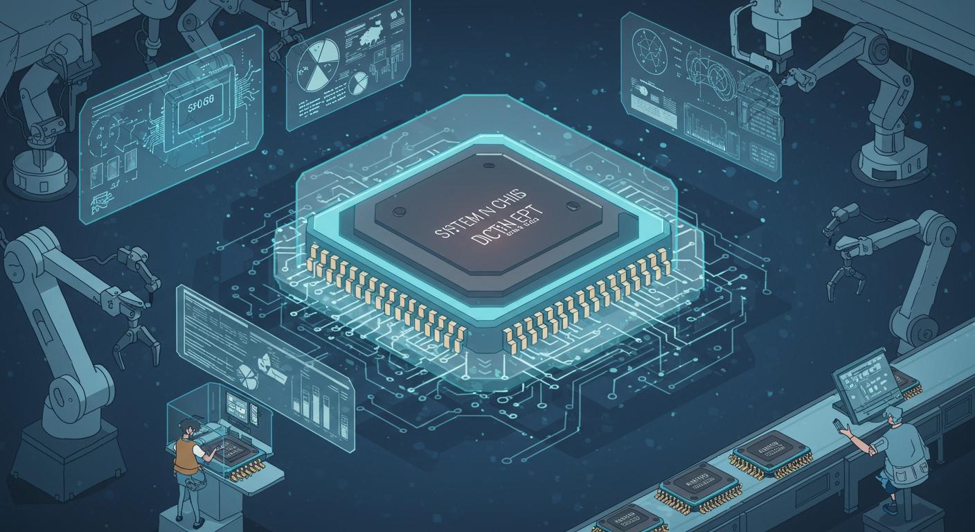
Engineers create a System on Chip (SoC) through a structured, multi-stage journey. This development involves three core stages that take an idea from a digital blueprint to a physical product.
The Three Core Stages of SoC Creation ⚙️
- Digital Design: Creating the architectural blueprint.
- Fabrication: Building the physical chip on silicon.
- Assembly & Testing: Finalizing and verifying the product.
Think of the SoC development process like constructing a skyscraper. The initial design must account for billions of components, like the 16 billion transistors in an Apple A16 Bionic system-on-chip. This complex development fuels a massive global market, which is projected to grow from USD 188.7 billion in 2024.

Key Takeaways
- Engineers create a System on Chip (SoC) in three main steps: design, fabrication, and assembly with testing.
- The design step is like drawing a detailed blueprint for the chip, deciding what it will do and how it will work.
- Fabrication is building the chip on a silicon wafer, using special tools to make tiny parts and connections.
- The final step involves testing the chip to find any problems, then packaging it safely for use in devices.
STAGE 1: THE SYSTEM ON CHIP DESIGN PHASE
The design phase is the first and most critical part of the SoC development journey. Engineers create a detailed digital blueprint for the entire system on chip. This stage defines every aspect of the chip's functionality, from its core logic to its software interfaces, setting the foundation for the physical product. The entire design workflow must manage immense complexity.
DEFINING THE SOC ARCHITECTURE
Engineers first define the SoC architecture. This architectural design is the high-level plan. It specifies the chip's purpose, features, and performance targets. The team makes key decisions about the processor cores, such as choosing between ARM or RISC-V architectures. They also select standard interfaces, like Arm's AMBA, to ensure all components communicate correctly. A primary goal of the SoC architecture is balancing performance with power consumption. Techniques like Dynamic Voltage and Frequency Scaling help achieve this balance. This initial design establishes the complete structure for the SoC.
RTL DESIGN AND IP CORE INTEGRATION
Next, the architectural design moves into Register-Transfer Level (RTL) design. Engineers use Hardware Description Languages (HDLs) like Verilog or VHDL to describe the chip's behavior. Modern SoC development relies heavily on pre-designed Intellectual Property (IP) blocks. These IP cores are like digital building blocks for functions such as USB or memory controllers.
What is an IP Core? 🧩 An IP core is a reusable, pre-verified unit of logic or a chip layout design. Companies like Arm and Synopsys are major IP providers. Using IP speeds up development and reduces risk.
The IP integration process connects these various IP blocks to form the complete SoC design. This approach is essential for managing the high design complexity of a modern system-on-chip.
SIMULATION AND VERIFICATION
Before manufacturing, the SoC design undergoes extensive simulation and verification. This step is crucial for finding and fixing bugs. The cost of a single error found after production, requiring a "respin," can exceed $10 million for an advanced chip. The verification and validation process uses powerful Electronic Design Automation (EDA) tools from companies like Synopsys and Cadence.
- Verification frequently consumes over 70% of the total project time.
- Validation teams often make up more than 70% of the entire design team.
This intense verification and validation effort ensures the design is correct, saving millions in potential costs and accelerating the development timeline. The soc design flow depends on this rigorous testing.
STAGE 2: FABRICATION - FROM BLUEPRINT TO SILICON
The fabrication stage transforms the digital SoC design into a physical reality. This highly complex process occurs inside a semiconductor fabrication plant, or "fab." Building a modern fab is a massive investment, with costs for a single facility exceeding $20 billion. Companies like TSMC, Samsung, and Intel operate these advanced plants, which are the heart of the entire electronics industry. The complex development of a modern SoC relies on these incredible facilities.
WAFER PRODUCTION
Fabrication begins with an ultra-pure silicon wafer. Engineers create large, single-crystal silicon ingots using the Czochralski process. These ingots, which can be up to two meters long, are then sliced into thin discs. Modern fabs primarily use 300 mm diameter wafers. This large size allows more chips to be produced per wafer, improving manufacturing efficiency for the SoC development process. Each wafer serves as the foundation for hundreds or thousands of individual SoC dies.
PHOTOLITHOGRAPHY AND ETCHING
Next, photolithography transfers the intricate circuit design onto the wafer. The process uses light to project the SoC design pattern onto a light-sensitive material called a photoresist.
Advanced Lithography 💡 For cutting-edge chips smaller than 7nm, manufacturers use Extreme Ultraviolet (EUV) lithography. Its extremely short wavelength enables the creation of much smaller and more complex features.
After exposing the pattern, etching removes unwanted material. Technicians use either wet etching with liquid chemicals or dry etching with plasmas to carve the circuit design into the silicon layer.
DEPOSITION AND ION IMPLANTATION
Engineers build the SoC layer by layer through deposition. Techniques like Atomic Layer Deposition (ALD) allow for the creation of incredibly thin, uniform films with atomic-level precision. Following deposition, ion implantation alters the silicon's electrical properties. This process shoots dopant atoms, like boron or arsenic, into the silicon. This doping creates the n-type and p-type regions that are essential for transistor function. This part of the development is critical for the final chip's performance.
METALLIZATION
The final fabrication step is metallization. This process creates a complex web of tiny copper wires that connect the billions of transistors on the system on chip. After each metal layer is deposited, a process called Chemical-Mechanical Planarization (CMP) polishes the surface perfectly flat. This ensures each new layer in the SoC design can be built correctly. This intricate wiring completes the physical structure of the SoC, turning the initial design into a functional circuit. The entire development journey depends on this precision.
STAGE 3: FINALIZING THE SYSTEM-ON-CHIP
The final stage of SoC development transforms the tested silicon wafers into finished products. This phase involves testing, cutting, packaging, and final verification to ensure each chip is ready for use in a device. The entire development process depends on the precision of these last steps.
WAFER TESTING AND DICING
Before cutting the wafer, engineers perform comprehensive electrical tests. This process finds faulty dies early, saving time and money. The testing flow checks for different types of failures.
- Wafer Probing: A probe card makes electrical contact with each die on the wafer. It checks for basic issues like short circuits.
- Die Test: This more detailed test verifies that the internal circuits of the SoC function correctly.
After testing, the wafer is cut into individual chips, or dies. Technicians use highly precise tools for this dicing process. Common methods include using a high-speed diamond blade or a focused laser beam to separate each SoC.
DIE PACKAGING
Next, each functional die goes into a protective package. This package shields the delicate silicon from physical damage and moisture. It also provides the electrical connections that link the SoC to a device's main circuit board. The package design uses several materials. Epoxy compounds encapsulate the die, while metal substrates provide support and help manage heat.
Different packaging technologies offer trade-offs between cost and performance.
| Package Type | Best For | Key Feature |
|---|---|---|
| BGA | Cost-sensitive products | A mature and reliable design |
| FCBGA | High-performance SoCs | Superior speed and thermal handling |
Choosing the right package is a critical part of the system-on-chip design. This choice directly impacts the final performance.
FINAL PRODUCT TESTING
The packaged SoC undergoes one last round of rigorous testing. A key part of this final verification is "burn-in" testing. This is an accelerated stress test to find any hidden defects.
What is Burn-in Testing? 🔥 Burn-in testing operates the SoC at high temperatures and voltages. This process simulates years of use in just a few hours. It helps eliminate chips that might fail early in their life, a problem known as "infant mortality."
This intense testing ensures that every system on chip leaving the factory is reliable and meets its design specifications. This final step concludes the complex SoC development journey.
The SoC development process guides a concept from digital design, through fabrication, to final testing. This journey transforms an idea into a physical system on chip, a monumental feat of engineering. The future of this process is already here.
The Next Wave of SoC Design 🚀 The next generation of SoC design integrates powerful AI accelerators. This enables advanced IoT devices and smartphones to run complex machine learning tasks locally, driving innovation in our connected world.
This intricate system-on-chip design is the engine powering modern technology, from data centers to the devices in our hands.
FAQ
What is the difference between a CPU and an SoC?
A CPU is the central processing unit, the "brain" of a computer. An SoC, or System on Chip, is a complete computer system. It integrates a CPU along with other essential components like a GPU, memory, and I/O controllers onto a single piece of silicon.
Why is SoC development so expensive?
The development process requires huge investments. Building a fabrication plant costs billions of dollars. The design phase uses costly software tools and large engineering teams. The entire journey from design to manufacturing demands extreme precision and specialized equipment, making it a very expensive undertaking.
How long does it take to create an SoC?
The complete SoC development cycle is a long process. From the initial concept to a market-ready product, the timeline typically spans from 18 to 24 months. More complex and advanced chip designs can extend this development period even further.
What programming languages do engineers use for SoC design?
Engineers use different languages for hardware and software.
Hardware vs. Software Languages 💻 Hardware Description Languages (HDLs) like
VerilogandVHDLdefine the chip's physical logic and structure. For software, engineers write firmware and drivers using languages like C, C++, and Assembly.