A Deep Dive into How a MOSFET Works
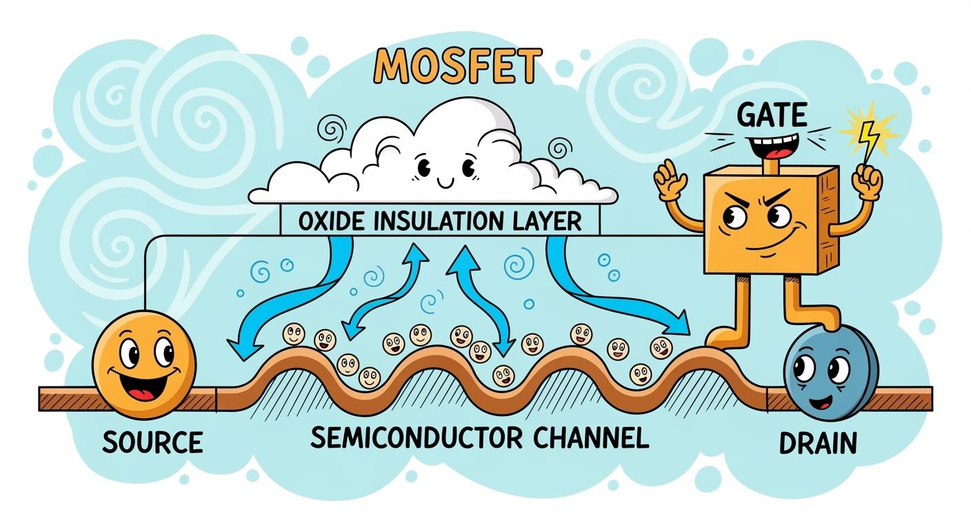
A metal-oxide-semiconductor field-effect transistor (MOSFET) is a unique transistor. A MOSFET acts as a voltage-controlled switch, unlike devices that rely on current. The MOSFET uses a specific voltage at its gate terminal to operate. The gate is the key.
A MOSFET is like a digital water valve. The gate is the control handle. The voltage applied to the gate determines if current can flow. A high voltage on the gate opens the path for current. A low voltage on the gate stops the current.
This voltage control at the gate means the MOSFET draws almost no input current, making all mosfets highly efficient. The gate voltage is the only control needed for the mosfet. The growing market for mosfets, including the popular n-channel mosfet and p-channel mosfet, highlights their importance. The mosfet is a fundamental component in modern electronics.
Metric | Value |
|---|---|
Market Size (2021) | USD 30,493.20 million |
Projected Market Size (2029) | USD 45,396.75 million |
Compound Annual Growth Rate (CAGR) | 5.10% |
Forecast Period | 2022-2029 |
Key Takeaways
A MOSFET is a special switch. It uses voltage at its gate to control current. This makes it very efficient.
MOSFETs have four parts: Gate, Drain, Source, and Body. The Gate acts like a handle to turn the current on or off.
The MOSFET works in three ways: off (cutoff), like a resistor (triode), or like a constant current source (saturation).
There are different types of MOSFETs. N-channel MOSFETs are common because they are faster and more efficient.
Important numbers for a MOSFET include the voltage needed to turn it on (threshold voltage) and how much it resists current when on (on-resistance).
How a MOSFET Controls Current
Understanding how a MOSFET controls current begins with its physical structure. The device's clever construction allows a voltage at one terminal to manage a large current flow between two other terminals. This control mechanism is central to the functioning of all mosfets. The correct mosfet biasing ensures the device performs as intended.
The Four Terminals: Gate, Drain, Source, and Body
A single mosfet has four connection points, or terminals. Each one has a specific job. The proper operation of the mosfet depends on these terminals working together.
Gate (G): This is the control terminal. Applying a voltage to the gate determines if the mosfet turns on or off. The gate acts like a switch handle.
Drain (D): This is the terminal where the main current exits the device. It is typically connected to a higher voltage potential than the source in an N-channel mosfet.
Source (S): This is the terminal where the main current enters the device. The source provides the charge carriers (electrons or holes) that flow to the drain.
Body (B): Also called the substrate, this is the base material of the transistor. In many applications, the body is connected directly to the source terminal, simplifying the mosfet to a three-terminal device.
The Insulated Gate: Metal-Oxide-Semiconductor
The name "MOSFET" describes its core structure: Metal-Oxide-Semiconductor. This layering is the key to its efficient operation. A thin layer of insulating material separates the gate from the rest of the transistor. This design is fundamental to the functioning of modern mosfets.
Note: The gate oxide layer is incredibly thin, often around 30 nanometers. This thinness is crucial, but the layer's insulating property gives the mosfet an extremely high input impedance. This means the gate draws almost no current, making the mosfet a very efficient voltage-controlled device.
The materials used for these layers have evolved, but the principle remains the same. The table below shows typical materials for each component in standard mosfets.
Component | Typical Materials |
|---|---|
Gate | Polysilicon, Metal |
Oxide Layer | Silicon Dioxide (SiO2) |
Semiconductor | Silicon (Si) |
This insulated gate structure is what allows the voltage at the gate to control the current between the source and drain without any direct electrical connection.
Forming the Channel and the Pinch-Off Effect
The magic of a mosfet happens in a region called the channel. In an N-channel mosfet, the body is made of P-type silicon, which has a surplus of positive charge carriers (holes). The source and drain regions are N-type silicon, with a surplus of negative electrons.
When a positive voltage is applied between the gate and source, it creates an electric field across the oxide layer. This field does two things:
It pushes the positive holes away from the area under the gate.
It attracts free electrons from the source and drain regions to the area under the gate.
If the gate voltage is strong enough to pass a certain point, called the threshold voltage (Vth), enough electrons gather to form a thin conductive path. This path is the inversion layer, or channel. It connects the source to the drain, allowing current to flow. The mosfet biasing must provide this gate voltage for operation.
As the voltage at the drain increases, the channel's shape changes. The electric field near the drain becomes stronger, which narrows the channel at that end. This leads to a condition called the pinch-off effect.
The conducting channel narrows significantly near the drain.
The current flow begins to level off, or saturate.
The mosfet operation transitions from behaving like a resistor to behaving like a constant current source.
Once pinch-off occurs, increasing the drain voltage further does not significantly increase the current. The current is now primarily controlled by the gate voltage. This is a vital part of mosfet biasing for amplifier circuits.
From Cutoff to Saturation: The Operating Regions
A mosfet operates in one of three distinct regions, depending on the gate-to-source voltage (VGS) and drain-to-source voltage (VDS). Proper mosfet biasing selects the correct region for a given application. The operation of all mosfets falls into these categories.
Cutoff Region
Condition: The gate voltage is less than the threshold voltage (
VGS < Vth).Behavior: No inversion channel forms between the source and drain. The mosfet is OFF, and almost no current flows from the drain to the source. This is the state used for a digital "0" or an open switch.
Triode (or Linear) Region
Condition: The gate voltage is greater than the threshold voltage (
VGS > Vth), and the drain voltage is low.Behavior: A channel exists, and the mosfet acts like a voltage-controlled resistor. The drain current is proportional to both the gate voltage and the drain voltage. This region is useful for creating electronically controlled switches or variable resistors.
Saturation Region
Condition: The gate voltage is greater than the threshold voltage (
VGS > Vth), and the drain voltage is high enough to cause pinch-off.Behavior: The drain current becomes nearly independent of the drain voltage. Instead, the current is controlled almost exclusively by the gate voltage. The mosfet acts as a constant current source. This is the primary region for analog amplification and a key part of mosfet biasing for that purpose.
Understanding these regions is essential for designing circuits with mosfets, as each region offers unique electrical characteristics for different applications.
The Main Types of MOSFETs
Not all mosfets are the same. Designers choose from several types based on their circuit's needs. The two main classifications for mosfets relate to their channel structure and the type of charge carrier they use. Understanding these differences is key to the proper functioning of any electronic device using a mosfet. The correct mosfet ensures efficient operation.
Enhancement-Mode vs. Depletion-Mode
The first major distinction is between enhancement-mode and depletion-mode mosfets. This difference lies in their default state. An enhancement-mode mosfet is normally off. It requires a gate voltage to create a channel and allow current to flow from the source to the drain. Most mosfets used today are enhancement types, especially in digital logic and power switching.
A depletion-mode mosfet is the opposite. It is normally on. A channel already exists, allowing current to flow without any gate voltage. Applying a voltage to the gate reduces, or depletes, the channel to turn the mosfet off. This unique operation makes depletion mosfets useful as current sources.
Depletion-Mode MOSFET | Enhancement-Mode MOSFET | |
|---|---|---|
Default State | Normally ON (current flows) | Normally OFF (no current) |
Gate Function | Gate voltage turns it OFF | Gate voltage turns it ON |
Channel | Built-in during manufacturing | Induced by gate voltage |
The functioning of enhancement and depletion mosfets is fundamentally different. The enhancement mosfet needs a gate voltage to "enhance" the channel. The depletion mosfet uses a gate voltage to "deplete" its existing channel. This makes depletion mosfets suitable for specialized analog circuits, while enhancement mosfets dominate applications like DC-DC converters and motor controllers.
N-Channel vs. P-Channel Charge Carriers
The second classification involves the charge carriers. An n-channel mosfet uses electrons to conduct current between its source and drain. A p-channel mosfet uses "holes" (the absence of electrons) for current conduction. This choice affects the mosfet's performance.
Electrons move much more easily through silicon than holes. This higher mobility gives the n-channel mosfet significant advantages. It has lower resistance and can switch current faster. For this reason, engineers often prefer an n-channel mosfet for high-current applications. The p-channel mosfet is still useful, especially for simplifying the gate drive circuit. The schematic symbol for these mosfets shows an arrow at the source. The arrow's direction indicates the mosfet type and the direction of conventional current flow.
Choosing the Right Type for Your Application
Selecting the right mosfet involves balancing performance and circuit simplicity. The choice between enhancement and depletion modes is often clear. Enhancement mosfets are the standard for switches. Depletion mosfets serve niche roles.
The choice between N-channel and P-channel mosfets depends on the switching configuration.
Low-Side Switch: An N-channel mosfet is ideal. Its source connects to ground, and a simple logic-level voltage at the gate can control a large current to the drain.
High-Side Switch: A P-channel mosfet often simplifies the design. Its source connects to the input voltage, and pulling the gate to a low voltage turns it on.
While a P-channel mosfet is simpler for high-side switching, it is less efficient. An N-channel mosfet can be used in a high-side configuration for better performance, but it requires a more complex gate driver circuit to supply the necessary gate voltage. The final decision depends on the specific demands of the mosfet operation.
Key Operating Characteristics
To use a MOSFET effectively, designers must understand its key datasheet parameters. These characteristics define how a specific MOSFET will behave in a circuit. They help engineers select the right mosfets for any application. The performance of all mosfets depends on these values.
Threshold Voltage (VGS(th))
The threshold voltage is the minimum gate-to-source voltage needed to turn a MOSFET on. Below this voltage, the mosfet remains off, and no current flows. The threshold voltage is a critical parameter for ensuring a mosfet activates correctly. The gate voltage must exceed the threshold voltage.
Standard MOSFETs: These mosfets often need a gate voltage around 10V to turn on fully.
Logic-Level MOSFETs: These mosfets are designed to work with lower voltages, often 5V or less. This allows direct control from microcontrollers.
A device's threshold voltage is not constant. The threshold voltage of a mosfet generally decreases as its temperature increases. This change is important in circuits with a low supply voltage. The gate must always provide a sufficient voltage above the threshold voltage. Many mosfets have a specific threshold voltage.
On-Resistance (RDS(on))
On-resistance is the resistance between the drain and source when the mosfet is fully on. A lower on-resistance means less power is lost as heat, making the mosfet more efficient. The gate-to-source voltage directly impacts this value. As the gate voltage increases well above the threshold voltage, the on-resistance of the mosfet decreases. This allows more current to flow efficiently from the source. Datasheets for mosfets specify this value at a certain gate voltage.
Gate Capacitance (CGS, CGD)
A mosfet has internal capacitances between its terminals. The gate-to-source (CGS) and gate-to-drain (CGD) capacitances are the most important. These are not added components; they are a natural part of the mosfet structure. To turn the mosfet on or off, a gate driver must charge or discharge these capacitances.
The gate-to-drain capacitance is especially significant. It causes the "Miller effect," which can slow down the switching speed. This capacitance creates a feedback path that increases the total capacitance seen at the gate, requiring more current from the driver.
Faster switching requires mosfets with lower gate capacitance. The gate needs a certain charge to reach the required voltage.
Breakdown Voltage (VDS(max))
The breakdown voltage is the maximum voltage a mosfet can handle between its drain and source terminals when it is off. Exceeding this voltage can cause permanent damage. This failure is called avalanche breakdown. A large, uncontrolled current flows from the drain to the source, which can destroy the mosfet. Designers must always choose mosfets with a breakdown voltage rating higher than any voltage they will experience in the circuit. This ensures the reliability of all mosfets.
A mosfet is a voltage-controlled switch. Its insulated gate uses an electric field from a gate voltage to control a channel. This makes the mosfet highly efficient. Designers choose between different mosfets. The choice of mosfet, like an N-channel mosfet, is fundamental. For any mosfet, key specs matter. The gate voltage must exceed the threshold voltage. A low on-resistance for a mosfet is also important. Every mosfet has a specific gate requirement. That mosfet needs the right gate voltage to operate its gate. The mosfet is a key component.
FAQ
Why are N-channel MOSFETs more common?
N-channel MOSFETs use electrons to conduct current. Electrons move through silicon much faster than the "holes" in P-channel devices. This speed gives N-channel MOSFETs lower resistance and higher efficiency. For this reason, designers often choose them for high-current switching applications.
What is the difference between a MOSFET and a BJT?
A MOSFET is a voltage-controlled device. A voltage at its gate controls the current flow. A Bipolar Junction Transistor (BJT) is a current-controlled device. A small current at its base terminal controls a larger current. MOSFETs are typically more efficient.
Why is the body terminal often connected to the source?
Connecting the body to the source simplifies the MOSFET into a three-terminal component. This common practice prevents the internal body diode from turning on unexpectedly. It ensures predictable behavior and makes the device easier to implement in most circuits.