Getting Started With The LM324 Operational Amplifier
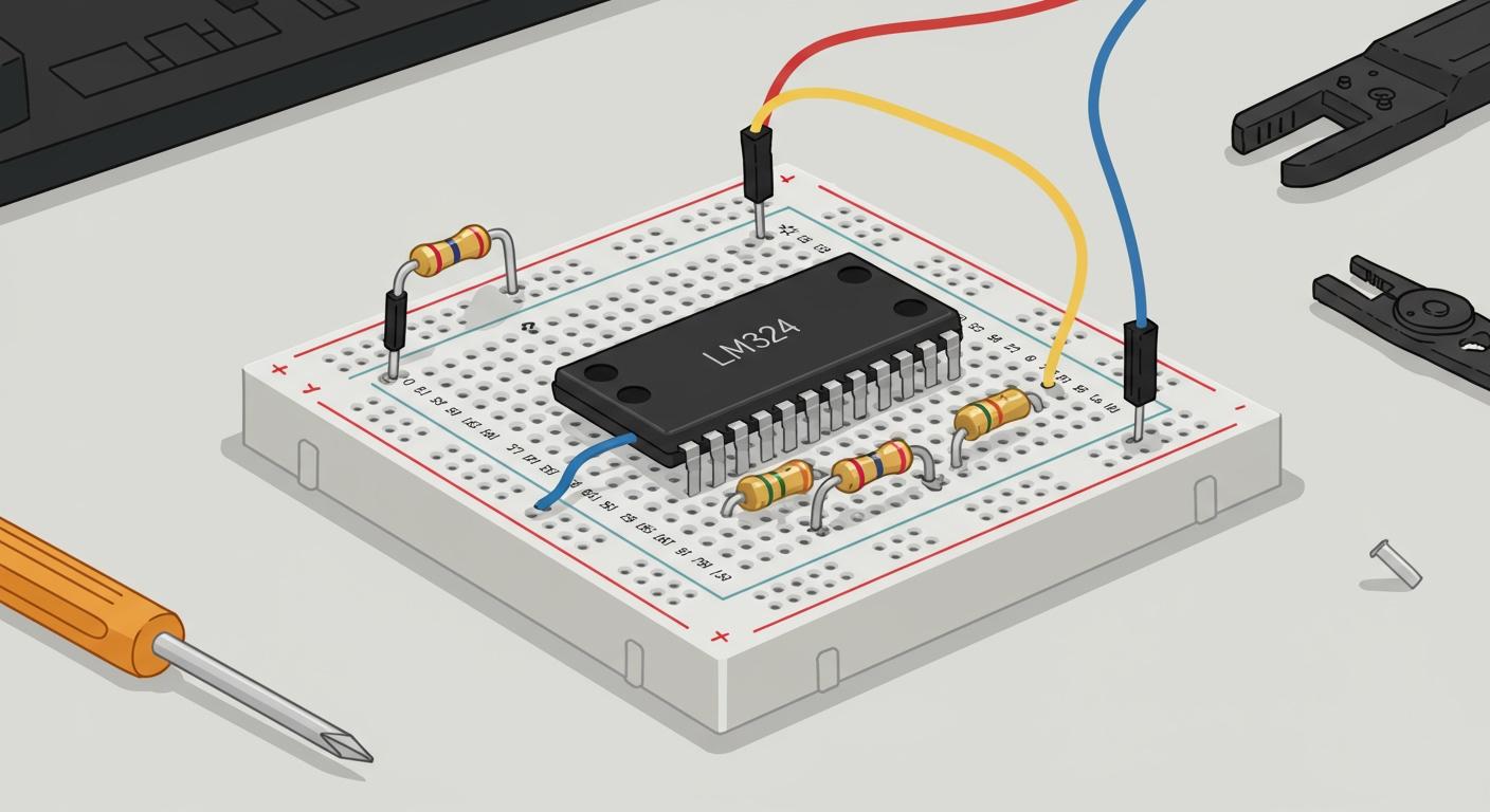
The LM324 is a low-cost, quad operational amplifier. It provides a power-efficient solution for a wide range of analog applications. The LM324 integrated circuit contains four independent, high-gain operational units.
This quad design makes the LM324 essential for diverse applications. It handles industrial signal conditioning and improves audio signal quality in sound equipment. The flexible operational nature of this amplifier makes the LM324 a reliable choice. The LM324 operational amplifier is a true workhorse component.
Key Takeaways
- The LM324 is a low-cost chip. It has four amplifiers. It works well for many basic electronic projects.
- This chip uses very little power. It can run on a single battery. This makes it good for portable devices.
- The LM324 is best for slow signals. It is not ideal for high-quality audio. It works well for things like sensors.
- You can use the LM324 for many tasks. These include making signals stronger or comparing voltages. It helps connect different parts of a circuit.
Key Features of the LM324
The LM324 operational amplifier offers several key features for electronics projects. These features make the LM324 a popular choice for many applications. Its design provides a balance of performance and efficiency. Understanding these advanced features helps designers use the quad amplifier effectively. The following sections explore the core features of this versatile IC.
Quad Amplifier Design
The LM324 contains four independent operational amplifiers in a single package. This quad design has significant benefits.
- Space-Saving: The quad layout reduces the total number of components. This saves valuable space on a printed circuit board (PCB). A single LM324 can manage a multi-channel signal path. Each channel can perform a different task.
- Cost-Effective: Using one quad chip is cheaper than using four separate amplifier chips. This lowers the cost for both prototypes and mass production. Each channel in the quad package works independently.
Flexible Power Supply
One of the best features of the LM324 is its flexible power supply range. It operates on a single power supply from 3V to 32V. This wide range makes it perfect for battery-powered devices.
- Portable audio devices can use a single channel for simple amplification.
- Sensor signal conditioning circuits amplify weak signals in remote monitoring systems.
- Battery-powered monitoring systems can run for a long time thanks to the chip's efficiency.
Low Power Consumption
The LM324 is known for its low power consumption. The entire quad package draws a very small supply current, typically around 700 µA. This low power consumption is a major advantage. The current draw stays nearly constant across the entire voltage range. This consistent performance makes low power consumption a reliable feature. The low power consumption per channel is about one-fifth that of older designs like the MC1741.
General-Purpose Operational Use
The LM324 is a true workhorse for general-purpose operational tasks. It excels at processing a DC signal in low-frequency applications. It is a great choice for industrial signal conditioning and instrumentation. However, its performance has limits. The chip is not ideal for high-quality audio due to noise and distortion. These advanced features show its specific strengths.
💡 LM324 vs. TL074: A Quick Comparison The table below shows how the LM324 quad operational amplifier compares to another popular quad chip, the TL074. This highlights the best use cases for each.
| Feature | LM324 | TL074 (Audio-Focused) |
|---|---|---|
| Supply Type | Excellent for single-supply | Best with dual-supply |
| Input Range | Works down to ground (0V) | Needs space from negative rail |
| Best Use | Slow DC signal processing | Faster AC signal (audio) |
| Distortion | Noticeable crossover distortion | Better performance for audio |
| Power | Very low power consumption | Higher power usage |
The LM324 Integrated Circuit Pinout
The lm324 integrated circuit typically comes in a 14-pin package. This pin configuration remains consistent across different package types, making the design process predictable. Common packages include:
- DIP (Dual In-line Package) for breadboarding.
- SOIC (Small Outline Integrated Circuit) for surface-mounting.
- TSSOP (Thin Shrink Small Outline Package) for compact designs.
Each pin has a specific role for one of the four operational amplifiers inside the lm324. The table below maps each pin to its function.
| Pin | Function | Description |
|---|---|---|
| 1 | 1OUT | Output of Amplifier 1 |
| 2 | 1IN- | Inverting Input of Amplifier 1 |
| 3 | 1IN+ | Non-inverting Input of Amplifier 1 |
| 4 | VCC | Positive Power Supply (+3V to +32V) |
| 5 | 2IN+ | Non-inverting Input of Amplifier 2 |
| 6 | 2IN- | Inverting Input of Amplifier 2 |
| 7 | 2OUT | Output of Amplifier 2 |
| 8 | 3OUT | Output of Amplifier 3 |
| 9 | 3IN- | Inverting Input of Amplifier 3 |
| 10 | 3IN+ | Non-inverting Input of Amplifier 3 |
| 11 | GND | Ground (Negative Power Supply) |
| 12 | 4IN+ | Non-inverting Input of Amplifier 4 |
| 13 | 4IN- | Inverting Input of Amplifier 4 |
| 14 | 4OUT | Output of Amplifier 4 |
Power Supply Pins
The lm324 requires a power source to function. Pin 4 (VCC) connects to the positive supply voltage, while Pin 11 (GND) connects to ground.
💡 Pro Tip: For stable operation, place a 0.1 µF (or 100nF) decoupling capacitor between VCC and GND. This capacitor should be physically close to the lm324 pins to filter out power supply noise.
Amplifier Input Pins
Each operational amplifier has two inputs. The inverting input (IN-) and the non-inverting input (IN+). For example, Amplifier 1 uses Pin 2 (1IN-) and Pin 3 (1IN+). The lm324 excels in single-supply systems because its input voltage range includes ground (0V). The input voltage should never exceed the supply voltage.
Amplifier Output Pins
Each amplifier has one output pin. This pin delivers the processed signal. Amplifier 1 uses Pin 1 (1OUT) for its output. The output voltage of the lm324 can swing close to the power rails but does not reach them completely. With a 30V supply, the output can typically reach up to 26V. This characteristic is important for circuit design.
Core LM324 Specifications
Understanding the electrical characteristics of the lm324 is key to designing effective circuits. These specifications define the operational limits and performance of the amplifier. The table below provides a quick reference to the most important values found in the datasheet.
| Specification | Typical Value | Description |
|---|---|---|
| Supply Voltage (VCC) | 3V to 32V (Single) | Wide range for battery or mains power. |
| Supply Current (Icc) | 700 µA (Quiescent) | Extremely low power draw for all four amps. |
| Gain Bandwidth Product | 1 MHz | Defines the amplifier's frequency response. |
| Slew Rate | 0.5 V/µs | The max rate of output voltage change. |
| Input Offset Voltage | 3 mV | A small error voltage at the inputs. |
| Operating Temperature | -40°C to +85°C | Suitable for a wide range of environments. |
Voltage and Current
The lm324 operational amplifier is highly efficient. It operates on a single supply from 3V to 32V. This wide voltage range makes it very versatile. The chip also has a very low supply current. This excellent power performance makes the lm324 a great choice for battery-operated devices where energy conservation is critical.
Bandwidth and Slew Rate
The lm324 has a high gain bandwidth product of around 1 MHz. This figure suggests the amplifier's capability at different frequencies. However, the slew rate of 0.5 V/µs limits its high-frequency performance. A fast-changing signal, like a 1 MHz sine wave, requires the output to change faster than the slew rate allows. This causes signal distortion. Therefore, while the lm324 has a high gain bandwidth product, it performs best with slower DC or low-frequency AC signal applications. The overall performance is a trade-off between gain and frequency.
Input and Offset
For high-precision circuits, the input offset voltage is a critical factor. The lm324 features a low input offset voltage, typically around 3 mV. This small inherent error comes from tiny mismatches in the internal components. In sensor circuits, this offset can reduce the accuracy of a measurement signal.
💡 The lm324 includes offset null pins. An external potentiometer can connect to these pins to cancel the offset. This feature is vital for achieving high precision and is a reason why the lm324 is used in sensitive instruments. Correcting this error improves the overall performance and ensures a clean output signal. The low input offset voltage is a key feature for precision work.
LM324 Operational Amplifier Circuits
The true power of the lm324 integrated circuit shines when it is used in practical circuits. Its four operational units allow for a variety of configurations within a single chip. These circuits form the building blocks for countless electronic devices and systems. Understanding these fundamental setups is the first step toward designing more complex applications. The following sections explore some of the most common and useful circuits for the lm324.
Single-Supply Configuration
A key strength of the lm324 is its ability to run from a single power source. This simplifies designs for battery-powered devices and other applications where only one voltage is available. In a single-supply setup, the negative power pin (GND) connects to the circuit ground (0V). This is different from many other operational amplifier ICs that require both positive and negative voltages.
The table below outlines the differences between single-supply and dual-supply operational modes.
| Feature | Single-Supply Operation | Dual-Supply Operation |
|---|---|---|
| VCC Connection | Positive voltage (VCC) to pin 4 | Positive voltage (e.g., +5V) to pin 4 |
| Vee/GND Connection | Ground (GND) to pin 11 | Negative voltage (e.g., -5V) to pin 11 |
| Ground Reference | Ground (GND) is the negative rail | A common ground can be used if needed |
| Typical Voltage Range | 3V to 32V | ±1.5V to ±16V |
| Input Common-Mode Range | Extends to the negative rail (GND) | Typically does not extend to both rails |
⚠️ Important: The power polarity of the lm324 differs from some other ICs. Always double-check connections to avoid reverse polarity, which can damage the chip. This is crucial for both single and dual-supply applications.
Voltage Comparator Circuit
An operational amplifier can function as a voltage comparator. This circuit compares two input voltages and produces a high or low output signal. For the lm324, you connect one signal to the non-inverting input (IN+) and a reference voltage to the inverting input (IN-).
- If the signal at IN+ is higher than the reference at IN-, the output goes high (near VCC).
- If the signal at IN+ is lower than the reference at IN-, the output goes low (near GND).
While the lm324 can perform this task, it is not ideal for high-speed applications. An internal component called a compensation capacitor makes the amplifier stable but also slows it down. For fast-switching applications, a dedicated comparator IC is a better choice.
- LM339 (Dedicated Comparator): Features a faster response time, making it suitable for applications that demand quick voltage comparisons.
- LM324 (Op-Amp): Exhibits a slower response time. Its slew rate of 0.5 V/µs is often too slow for comparator applications above a few kilohertz, where it can distort the output signal.
This makes the lm324 suitable for slow-changing signal comparisons, like in a thermostat circuit, but not for fast applications like PWM signal generation.
Non-Inverting Amplifier
One of the most common typical applications for the lm324 operational amplifier is signal amplification. A non-inverting amplifier boosts the voltage of an input signal without changing its polarity. The circuit uses two external resistors to set the voltage gain. The formula for the gain is:
Gain = 1 + (R2 / R1)
Here, R2 is the feedback resistor (connecting the output to the inverting input), and R1 connects the inverting input to ground. For example, using R1 = 10kΩ and R2 = 90kΩ results in a voltage gain of 10. This configuration is excellent for boosting a weak sensor signal.
This amplifier design also offers a very high input impedance, typically around 2MΩ. This feature is a major benefit for signal sources with high output impedance. The high input impedance of the amplifier prevents it from drawing significant current from the source. This preserves the integrity of the original signal and prevents voltage drops, ensuring accurate amplification.
Voltage Follower (Buffer)
A voltage follower, or buffer, is a special type of non-inverting amplifier with a voltage gain of exactly 1. It is created by connecting the output pin directly to the inverting input pin. The input signal goes to the non-inverting input. The output signal will be an exact copy of the input signal.
So, why use an amplifier with no gain? The purpose is impedance transformation.
A voltage follower has a very high input impedance and a very low output impedance. This makes it perfect for isolating circuit stages. A common application is buffering the signal from a high-impedance sensor before it goes to an Analog-to-Digital Converter (ADC).
- A sensor may have a high output impedance, meaning it cannot supply much current.
- An ADC may have a lower input impedance, causing it to draw too much current from the sensor. This "loads" the sensor and changes its voltage, leading to an inaccurate reading.
- Placing an lm324 voltage follower between them solves the problem. The follower presents a high impedance to the sensor, preserving the signal. It then provides the same signal to the ADC from its own low-impedance output, which can supply the needed current. This is a simple yet powerful technique in many data acquisition applications.
The lm324 is an excellent starting point for electronics beginners. Its low cost and versatility make the lm324 widely available for many projects. Experienced engineers also value the lm324 as a reliable workhorse component. The lm324 excels in numerous general-purpose analog applications.
While the lm324 is a great all-rounder, other ICs offer specialized performance. For instance, the LM358 provides lower noise, and the LT1014 offers higher precision for sensitive applications. This makes the lm324 a foundational part for learning before exploring more advanced options.
FAQ
Can I use the LM324 for audio amplifiers?
The LM324 is not ideal for high-quality audio. It introduces noticeable crossover distortion, which can affect sound quality. Other op-amps, like the TL074 or NE5532, offer better performance for audio applications. The LM324 works best for low-frequency signals.
What is the difference between the LM324 and the LM358?
The LM324 and LM358 are very similar. The main difference is the number of amplifiers.
- LM324: Contains four op-amps (Quad).
- LM358: Contains two op-amps (Dual).
Both chips share similar electrical characteristics and are great for single-supply projects.
What should I do with unused op-amps in an LM324?
An unused op-amp can cause problems if its inputs are left floating. Designers should configure any unused op-amp as a voltage follower. Connect the output to the inverting input. Then, connect the non-inverting input to a stable voltage, like ground.
This configuration prevents the unused section from oscillating or drawing extra current. It ensures the entire chip operates predictably.
Can the LM324 output reach the power supply voltages?
No, the LM324 is not a rail-to-rail op-amp. Its output voltage cannot reach the full positive supply (VCC) or the negative supply (GND). The output typically swings to within about 1.5V of VCC and very close to GND in single-supply mode.